LM5045 www.ti.com SNVS699G – FEBRUARY 2011 – REVISED MARCH 2013 Full-Bridge PWM Controller with Integrated MOSFET Drivers Check for Samples: LM5045 FEATURES DESCRIPTION • The LM5045 PWM controller contains all of the features necessary to implement Full-Bridge topology power converters using either current mode or voltage mode control. This device is intended to operate on the primary side of an isolated dc-dc converter with input voltage up to 100V.
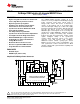
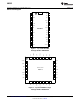
LM5045 SNVS699G – FEBRUARY 2011 – REVISED MARCH 2013 www.ti.com Connection Diagram UVLO VIN OVP HS1 RAMP HO1 BST1 CS SLOPE SR1 COMP LO1 REF PGND HTSSOP28 RT VCC AGND LO2 RD1 SR2 RD2 BST2 HO2 RES HS2 SS SSSR SS OFF Figure 1. Top View HTSSOP Package Number PWP0028A HO1 HS1 VIN UVLO OVP RAMP CS SLOPE BST1 COMP SR1 LO1 REF 5 mm x 5 mm PGND WQFN 28 RT AGND VCC RD1 LO2 RD2 SR2 BST2 HO2 HS2 SS OFF SSSR SS RES Figure 2.
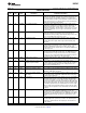
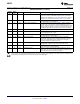
LM5045 www.ti.com SNVS699G – FEBRUARY 2011 – REVISED MARCH 2013 PIN DESCRIPTIONS HTSSOP Pin WQFN Pin Name 1 25 UVLO 2 26 OVP/OTP 3 27 RAMP 4 28 CS 5 1 6 Description Application Information Line Under-Voltage Lockout An external voltage divider from the power source sets the shutdown and standby comparator levels. When UVLO reaches the 0.4V threshold the VCC and REF regulators are enabled. At the 1.25V threshold, the SS pin is released and the controller enters the active mode.
LM5045 SNVS699G – FEBRUARY 2011 – REVISED MARCH 2013 www.ti.com PIN DESCRIPTIONS (continued) HTSSOP Pin WQFN Pin Name 15 11 SSOFF 19 15 21 17 Description Application Information Soft-Stop Disable When SS OFF pin is connected to the AGND, the LM5045 softstops in the event of a VIN UVLO and Hiccup mode current limit condition. If the SSOFF pin is connected to REF pin, the controller hard-stops on any fault condition. Refer Table 1 for more details.
LM5045 www.ti.com SNVS699G – FEBRUARY 2011 – REVISED MARCH 2013 Absolute Maximum Ratings (1) VIN to GND -0.3V to 105V HS to GND (2) -5V to 105V BST1/BST2 to GND -0.3V to 116V BST1/BST2 to HS1/HS2 HO1/HO2 to HS1/HS2 -0.3V to 16V (3) -0.3V to BST1/BST2+0.3V LO1/LO2/SR1/SR2 (3) -0.3V to VCC+0.3V VCC to GND -0.3V to 16V REF,SSOFF,RT,OVP,UVLO to GND -0.3V to 7V RAMP -0.3V to 7V COMP -0.3V COMP Input Current +10mA All other inputs to GND (3) -0.3 to REF+0.
LM5045 SNVS699G – FEBRUARY 2011 – REVISED MARCH 2013 www.ti.com Electrical Characteristics (continued) Limits in standard typeface are for TJ = 25°C only; limits in boldface type apply the junction temperature range of -40°C to +125°C. Unless otherwise specified, the following conditions apply: VIN = 48V, RT = 25kΩ, RD1=RD2=20kΩ. No load on HO1, HO2, LO1, LO2, SR1, SR2, COMP=0V, UVLO=2.5V, OVP=0V, SSOFF=0V. Symbol Parameter Conditions Min Typ Max REF Voltage IREF = 0mA 4.85 5 5.
LM5045 www.ti.com SNVS699G – FEBRUARY 2011 – REVISED MARCH 2013 Electrical Characteristics (continued) Limits in standard typeface are for TJ = 25°C only; limits in boldface type apply the junction temperature range of -40°C to +125°C. Unless otherwise specified, the following conditions apply: VIN = 48V, RT = 25kΩ, RD1=RD2=20kΩ. No load on HO1, HO2, LO1, LO2, SR1, SR2, COMP=0V, UVLO=2.5V, OVP=0V, SSOFF=0V.
LM5045 SNVS699G – FEBRUARY 2011 – REVISED MARCH 2013 www.ti.com Electrical Characteristics (continued) Limits in standard typeface are for TJ = 25°C only; limits in boldface type apply the junction temperature range of -40°C to +125°C. Unless otherwise specified, the following conditions apply: VIN = 48V, RT = 25kΩ, RD1=RD2=20kΩ. No load on HO1, HO2, LO1, LO2, SR1, SR2, COMP=0V, UVLO=2.5V, OVP=0V, SSOFF=0V.
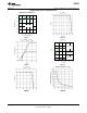
LM5045 www.ti.com SNVS699G – FEBRUARY 2011 – REVISED MARCH 2013 Typical Performance Characteristics Application Board Efficiency VCC vs ICC 100 36V EFFICIENCY (%) 90 48V 80 72V VOUT= 3.3V 70 60 50 5 10 15 20 25 LOAD CURRENT (A) 30 Figure 3. Figure 4. VVCC and VREF vs. VVIN IIN vs. VIN 6 5 VUVLO=3V IIN(V) 4 3 VUVLO=1V 2 1 VUVLO=0V 0 0 20 40 60 VIN(V) 80 Figure 5. Figure 6. VREF vs. IREF Oscillator Frequency vs. RT Figure 7. Figure 8.
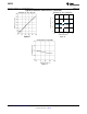
LM5045 SNVS699G – FEBRUARY 2011 – REVISED MARCH 2013 www.ti.com Typical Performance Characteristics (continued) Dead-Time T1, T2 vs. RD1, RD2 Dead-Time T1, T2 vs. Temperature DEAD-TIME T1,T2 (ns) 75 70 T2 65 T1 60 55 -50 Figure 9. 0 50 100 TEMPERATURE(°C) 150 Figure 10. CS Threshold vs. Temperature Figure 11.
LM5045 www.ti.com SNVS699G – FEBRUARY 2011 – REVISED MARCH 2013 Block Diagram VOLTAGE REGULATOR VIN 1.25V VCC + OVP UVLO 0.4V VCC UVLO 20 PA - 5V HYSTERESIS + SHUTDOWN + 1.
LM5045 SNVS699G – FEBRUARY 2011 – REVISED MARCH 2013 www.ti.com FUNCTIONAL DESCRIPTION The LM5045 PWM controller contains all of the features necessary to implement a Full-Bridge topology power converter using either current mode or voltage mode control. This device is intended to operate on the primary side of an isolated dc-dc converter with input voltage up to 100V.
LM5045 www.ti.com SNVS699G – FEBRUARY 2011 – REVISED MARCH 2013 Over Voltage Protection An external voltage divider can be used to set either an over voltage or an over temperature protection. During an OVP condition, the SS and SSSR capacitors are discharged and all the outputs are disabled. The divider must be designed such that the voltage at the OVP pin is greater than 1.25V when over voltage/temperature condition exists. Hysteresis is accomplished with an internal 20μA current source.
LM5045 SNVS699G – FEBRUARY 2011 – REVISED MARCH 2013 • • • • www.ti.com Once RES capacitor reaches 2.0V, threshold, the 10μA current source is turned-on again. The RES capacitor voltage is ramped between 4.0V and 2.0V eight times. When the counter reaches eight, the RES pin voltage is pulled low and the soft-start capacitor is released to begin a soft-start sequence. The SS capacitor voltage slowly increases. When the SS voltage reaches 1.0V, the PWM comparator will produce the first narrow pulse.
LM5045 www.ti.com SNVS699G – FEBRUARY 2011 – REVISED MARCH 2013 Ramp Pin The voltage at the RAMP pin provides the modulation ramp for the PWM comparator. The PWM comparator compares the modulation ramp signal at the RAMP pin to the loop error signal to control the duty cycle. The modulation ramp signal can be implemented either as a ramp proportional to the input voltage, known as feedforward voltage mode control, or as a ramp proportional to the primary current, known as current mode control.
LM5045 SNVS699G – FEBRUARY 2011 – REVISED MARCH 2013 www.ti.com Soft-Start The soft-start circuit allows the power converter to gradually reach a steady state operating point, thereby reducing the start-up stresses and current surges. When bias is supplied to the LM5045, the SS capacitor is discharged by an internal MOSFET. When the UVLO, VCC and REF pins reach their operating thresholds, the SS capacitor is released and is charged with a 20µA current source.
LM5045 www.ti.com SNVS699G – FEBRUARY 2011 – REVISED MARCH 2013 CLK HO1,LO2 Tonmax Tosc HO2,LO1 T1 T1 TOSC = 1 FOSC T1 D RD1 Figure 14. Timing Diagram Illustrating the Maximum Duty Cycle and Dead-Time Set by RD1 Synchronous Rectifier Control Outputs (SR1 & SR2) Synchronous rectification (SR) of the transformer secondary provides higher efficiency, especially for low output voltage converters, compared to the diode rectification. The reduction of rectifier forward voltage drop (0.5V 1.
LM5045 SNVS699G – FEBRUARY 2011 – REVISED MARCH 2013 www.ti.com HO1, LO2 SR2 T1 T2 HO2, LO1 SR1 T1 T2 Figure 15. Synchronous Rectifier Timing Diagram Soft-Start of the Synchronous Rectifiers In addition to the basic soft-start already described, the LM5045 contains a second soft-start function that gradually turns on the synchronous rectifiers to their steady-state duty cycle.
LM5045 www.ti.com SNVS699G – FEBRUARY 2011 – REVISED MARCH 2013 CLK HO2/LO1 HO1/LO2 SR1 T1 T2 SR2 Power Transfer T1 Freewheel Waveforms during soft-start A. Waveforms during Soft-Start B. Waveforms after Soft-Start T2 Waveforms after soft-start Figure 16. Pre-Bias Startup A common requirement for power converters is to have a monotonic output voltage start-up into a pre-biased load i.e. a pre-charged output capacitor.
LM5045 SNVS699G – FEBRUARY 2011 – REVISED MARCH 2013 www.ti.com 2.0V SS 1.0V Primary Secondary Bias COMP 1.0V SSSR SR1, SR2 VOUT Prebiased Load Figure 17. Pre-Bias Voltage Startup Waveforms Soft-Stop Off The Soft-Start Off (SSOFF) pin gives additional flexibility by allowing the power converter to be configured for hard-stop during line UVLO and hiccup mode condition. If the SS OFF pin is pulled up to the 5V REF pin, the power converter hard-stops in any fault condition.
LM5045 www.ti.com SNVS699G – FEBRUARY 2011 – REVISED MARCH 2013 Table 1. Soft-Stop in Fault Conditions (1) (1) Fault Condition SSSR UVLO (UVLO<1.25V) Soft-Stop 3x the charging rate OVP (OVP>1.25V) Hard-Stop Hiccup (CS>0.75 and RES>1V) Soft-Stop 6x the charging rate VCC/VREF UV Hard-Stop Internal Thermal Limit Hard-Stop Note: All the above conditions are valid with SSOFF pin tied to GND. If SSOFF=5V, the LM5045 hard-stops in all the conditions.
LM5045 SNVS699G – FEBRUARY 2011 – REVISED MARCH 2013 SLOPE PROPORTIONAL TO VIN www.ti.com VIN 5V COMP RFF VIN 5k R R 1V Gate Drive 1:1 RAMP CLK CFF LM5045 Figure 19. Feed-Forward Voltage Mode Configuration The recommended capacitor value range for CFF is from 100pF to 1800pF. Referring to Figure 19, it can be seen that CFF value must be small enough to be discharged with in the clock pulse-width which is typically within 50ns. The RDS(ON) of the internal discharge FET is 5.5Ω.
LM5045 www.ti.com SNVS699G – FEBRUARY 2011 – REVISED MARCH 2013 VIN and VCC The voltage applied to the VIN pin, which may be the same as the system voltage applied to the power transformer’s primary (VPWR), can vary in the range of the 14 to 100V. It is recommended that the filter shown in Figure 21 be used to suppress the transients that may occur at the input supply. This is particularly important when VIN is operated close to the maximum operating rating of the LM5045.
LM5045 SNVS699G – FEBRUARY 2011 – REVISED MARCH 2013 www.ti.com 10V - 16V (from aux winding) VPWR VIN VCC LM5045 11V Figure 22. Start-up Regulator for VPWR>100V UVLO and OVP Voltage Divider Selection Two dedicated comparators connected to the UVLO and OVP pins are used to detect under voltage and over voltage conditions. The threshold values of both these comparators are set at 1.25V.
LM5045 www.ti.com SNVS699G – FEBRUARY 2011 – REVISED MARCH 2013 VPWR LM5045 R1 1.25V STANDBY UVLO 20 PA R2 0.4V SHUTDOWN Figure 23. Basic UVLO Configuration LM5045 5V VPWR 20 PA R1 OVP STANDBY 1.25V R2 Figure 24. Basic OVP Configuration VPWR R1 UVLO 1.25V STANDBY LM5045 20 PA 0.4V R2 SHUTDOWN 5V 20 PA OVP 1.25V STANDBY R3 Figure 25. UVLO/OVP Divider The UVLO and OVP can also be set together using a 3 resistor divider ladder as shown in Figure 25.
LM5045 SNVS699G – FEBRUARY 2011 – REVISED MARCH 2013 www.ti.com Figure 27 shows an application of the OVP comparator for Remote Thermal Protection using a thermistor (or multiple thermistors) which may be located near the main heat sources of the power converter. The negative temperature coefficient (NTC) thermistor is nearly logarithmic, and in this example a 100kΩ thermistor with the β material constant of 4500 Kelvin changes to approximately 2kΩ at 130ºC.
LM5045 www.ti.com SNVS699G – FEBRUARY 2011 – REVISED MARCH 2013 VPWR Q3 Q1 VIN NS1 RF CS NP LM5045 RCS CF NS2 AGND Q2 Q4 Figure 28. Transformer Current Sense Q3 Q1 NP Q4 Q2 VIN CS LM5045 RF CF RCS AGND Figure 29. Resistor Current Sense Hiccup Mode Current Limit Restart The operation of the hiccup mode restart circuit is explained in the FUNCTIONAL DESCRIPTION section. During a continuous current limit condition, the RES pin is charged with 30µA current source.
LM5045 SNVS699G – FEBRUARY 2011 – REVISED MARCH 2013 www.ti.com 4V 2V 1V Count to Eight Restart delay Soft-Start 1V Hiccup Mode off-time Figure 30. Hiccup Mode Delay and Soft-Start Timing Diagram Augmenting the Gate Drive Strength The LM5045 includes powerful 2A integrated gate drivers. However, in certain high power applications (>500W), it might be necessary to augment the strength of the internal gate driver to achieve higher efficiency and better thermal performance.
LM5045 www.ti.com SNVS699G – FEBRUARY 2011 – REVISED MARCH 2013 Depending on the gate charge characteristics of the primary FET, if it is required to speed up both the turn-on and the turn-off time, a bipolar totem pole structure as shown in Figure 32 can be used. When LO1 goes high, the gate to source current is sourced through the NPN transistor Q1 and similar to the circuit shown in Figure 31 when LO1 goes low, the PNP transistor Q2 expedites the turn-off process.
LM5045 SNVS699G – FEBRUARY 2011 – REVISED MARCH 2013 www.ti.com Printed Circuit Board Layout The LM5045 current sense and PWM comparators are very fast and respond to short duration noise pulses. The components at the CS, COMP, SLOPE, RAMP, SS, SSSR, RES, UVLO, OVP, RD1, RD2, and RT pins should be physically close as possible to the IC, thereby minimizing noise pickup on the PC board trace inductance. Eliminating or minimizing via’s in these critical connections are essential.
LM5045 www.ti.com SNVS699G – FEBRUARY 2011 – REVISED MARCH 2013 REVISION HISTORY Changes from Revision F (March 2013) to Revision G • Page Changed layout of National Data Sheet to TI format ..........................................................................................................
PACKAGE OPTION ADDENDUM www.ti.
PACKAGE OPTION ADDENDUM www.ti.
PACKAGE MATERIALS INFORMATION www.ti.com 11-Oct-2013 TAPE AND REEL INFORMATION *All dimensions are nominal Device Package Package Pins Type Drawing SPQ Reel Reel A0 Diameter Width (mm) (mm) W1 (mm) B0 (mm) K0 (mm) P1 (mm) LM5045MHX/NOPB HTSSOP PWP 28 2500 330.0 16.4 LM5045SQ/NOPB WQFN RSG 28 1000 178.0 LM5045SQX/NOPB WQFN RSG 28 4500 330.0 6.8 10.2 1.6 8.0 16.0 Q1 12.4 5.3 5.3 1.3 8.0 12.0 Q1 12.4 5.3 5.3 1.3 8.0 12.
PACKAGE MATERIALS INFORMATION www.ti.com 11-Oct-2013 *All dimensions are nominal Device Package Type Package Drawing Pins SPQ Length (mm) Width (mm) Height (mm) LM5045MHX/NOPB HTSSOP PWP 28 2500 367.0 367.0 35.0 LM5045SQ/NOPB WQFN RSG 28 1000 210.0 185.0 35.0 LM5045SQX/NOPB WQFN RSG 28 4500 367.0 367.0 35.
MECHANICAL DATA PWP0028A MXA28A (Rev D) www.ti.
MECHANICAL DATA RSG0028A SQA28A (Rev B) www.ti.
IMPORTANT NOTICE Texas Instruments Incorporated and its subsidiaries (TI) reserve the right to make corrections, enhancements, improvements and other changes to its semiconductor products and services per JESD46, latest issue, and to discontinue any product or service per JESD48, latest issue. Buyers should obtain the latest relevant information before placing orders and should verify that such information is current and complete.