
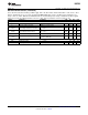
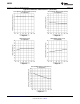
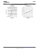
Datasheet

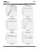

V
IN
V
OUT
STATUS
UVLO
OVP
TIMER
GND
EN
OUT
SENSE
GATE
VIN
LM5060
EN
GND GND
nPGD
High = Fault, Low= OK
High = On, Low= Off
LM5060
www.ti.com
SNVS628F –OCTOBER 2009–REVISED APRIL 2013
LM5060 High-Side Protection Controller with Low Quiescent Current
Check for Samples: LM5060
1
FEATURES
APPLICATIONS
2
• Available in Automotive Grade / AEC Q-100
• Automotive Body Electronics
• Wide Operating Input Voltage Range: +5.5V to • Industrial Power Distribution and Control
+65V
PACKAGE
• Less than 15 µA Quiescent Current in Disabled
Mode
• 10-Lead VSSOP
• Controlled Output Rise Time for Safe
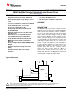
DESCRIPTION
Connection of Capacitive Loads
The LM5060 high-side protection controller provides
• Charge Pump Gate Driver for External N-
intelligent control of a high-side N-Channel MOSFET
Channel MOSFET
during normal on/off transitions and fault conditions.
• Adjustable Under-Voltage Lock-Out (UVLO)
In-rush current is controlled by the nearly constant
with Hysteresis
rise time of the output voltage. A power good output
• UVLO Serves as Second Enable Input for
indicates when the output voltage reaches the input
voltage and the MOSFET is fully on. Input Under-
Systems Requiring Safety Redundancy
Voltage Lock-Out, with hysteresis, is provided as well
• Programmable Fault Detection Delay Time
as programmable input Over-Voltage Protection. An
• MOSFET Latched off After Load Fault is
enable input provides remote On / Off control. The
Detected
programmable Under-Voltage Lock-Out input can be
used as second enable input for safety redundancy.
• Active Low Open Drain POWER GOOD (nPGD)
A single capacitor programs the initial start-up V
GS
Output
fault detection delay time, the transition V
DS
fault
• Adjustable Input Over-Voltage Protection
detection delay time, and the continuous Over-
(OVP)
Current V
DS
fault detection delay time. When a
• Immediate Restart After Over-Voltage
detected fault condition persists longer than the
Shutdown
allowed fault delay time, the MOSFET is latched off
until either the Enable input or the Under-Voltage
Lock-Out input is toggled low and then high.
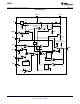
Typical Application
1
Please be aware that an important notice concerning availability, standard warranty, and use in critical applications of
Texas Instruments semiconductor products and disclaimers thereto appears at the end of this data sheet.
2All trademarks are the property of their respective owners.
PRODUCTION DATA information is current as of publication date.
Copyright © 2009–2013, Texas Instruments Incorporated
Products conform to specifications per the terms of the Texas
Instruments standard warranty. Production processing does not
necessarily include testing of all parameters.