
Datasheet

VDD LI
HI
VDD
HSHBHOHHOL
HS
LOH
LOL
VSS
A
B
C
D
1 2 3 4
Top View
VDD
LI
HI
VDD
HS HB HOH HOL
HS
LOH
LOL
VSS
A
B
C
D
1234
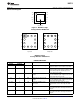
Bump Side
1
2
3
4
9
6
7
8
VDD
HB
HOH
HOL
HI
LI
VSS
LOH
HS
5
10
LOL
Exposed Pad
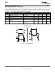
LM5113
www.ti.com
SNVS725F –JUNE 2011–REVISED APRIL 2013
Connection Diagram
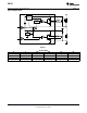
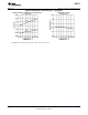
Figure 2. WSON Package
Package Number DPR0010A
DSBGA Package
Package Number YFX0012FLA
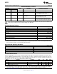
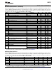
PIN DESCRIPTIONS
Pin Number Name Description Applications Information
DSBGA WSON-10
A3, C4
(1)
1 VDD 5V Positive gate drive supply Locally decouple to VSS using low ESR/ESL
capacitor located as close to the IC as possible.
D3 2 HB High-side gate driver bootstrap Connect the positive terminal of the bootstrap
rail capacitor to HB and the negative terminal to HS.
The bootstrap capacitor should be placed as
close to the IC as possible.
D2 3 HOH High-side gate driver turn-on Connect to the gate of high-side GaN FET with a
output short, low inductance path. A gate resistor can be
used to adjust the turn-on speed.
D1 4 HOL High-side gate driver turn-off Connect to the gate of high-side GaN FET with a
output short, low inductance path. A gate resistor can be
used to adjust the turn-off speed.
C1, D4
(1)
5 HS High-side GaN FET source Connect to the bootstrap capacitor negative
connection terminal and the source of the high-side GaN
FET.
B4 6 HI High-side driver control input The LM5113 inputs have TTL type thresholds.
Unused inputs should be tied to ground and not
left open.
A4 7 LI Low-side driver control input The LM5113 inputs have TTL type thresholds.
Unused inputs should be tied to ground and not
left open.
(1) A3 and C4, C1 and D4 are internally connected.
Copyright © 2011–2013, Texas Instruments Incorporated Submit Documentation Feedback 3
Product Folder Links: LM5113