
Datasheet

LM5113
SNVS725F –JUNE 2011–REVISED APRIL 2013
www.ti.com
PIN DESCRIPTIONS (continued)
Pin Number Name Description Applications Information
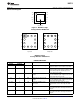
DSBGA WSON-10
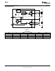
A2 8 VSS Ground return All signals are referenced to this ground.
A1 9 LOL Low-side gate driver sink-current Connect to the gate of the low-side GaN FET with
output a short, low inductance path. A gate resistor can
be used to adjust the turn-off speed.
B1 10 LOH Low-side gate driver source- Connect to the gate of high-side GaN FET with a
current output short, low inductance path. A gate resistor can be
used to adjust the turn-on speed.
EP Exposed Pad It is recommended that the exposed pad on the
bottom of the package be soldered to ground
plane on the PC board to aid thermal dissipation.
These devices have limited built-in ESD protection. The leads should be shorted together or the device placed in conductive foam
during storage or handling to prevent electrostatic damage to the MOS gates.
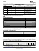
Absolute Maximum Ratings
(1)
VDD to VSS −0.3V to 7V
HB to HS −0.3V to 7V
LI or HI Input −0.3V to 15V
LOH, LOL Output −0.3V to VDD +0.3V
HOH, HOL Output V
HS
−0.3V to V
HB
+0.3V
HS to VSS −5V to +100V
HB to VSS 0 to 107V
HB to VDD 0 to 100V
Junction Temperature +150°C
Storage Temperature Range −55°C to +150°C
ESD Rating HBM 2 kV
(1) Absolute Maximum Ratings indicate limits beyond which damage to the component may occur. Operating Ratings are conditions under
which operation of the device is ensured. Operating Ratings do not imply ensured performance limits. For ensured performance limits
and associated test conditions, see the Electrical Characteristics tables.
Recommended Operating Conditions
VDD +4.5V to +5.5V
LI or HI Input 0V to +14V
HS −5V to 100V
HB V
HS
+4V to V
HS
+5.5V
HS Slew Rate <50 V/ns
Junction Temperature −40°C to +125°C
Electrical Characteristics
Limits in standard type are for T
J
= 25°C only; limits in boldface type apply over the junction temperature (T
J
) range of -40°C
to +125°C. Minimum and Maximum limits are ensured through test, design, or statistical correlation. Typical values represent
the most likely parametric norm at T
J
= 25°C, and are provided for reference purposes only. Unless otherwise specified, V
DD
=
V
HB
= 5V, V
SS
= V
HS
= 0V, No Load on LOL and HOL or HOH and HOL
(1)
.
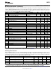
Symbol Parameter Conditions Min Typ Max Units
SUPPLY CURRENTS
I
DD
VDD Quiescent Current LI = HI = 0V 0.07 0.1 mA
I
DDO
VDD Operating Current f = 500 kHz 2.0 3.0 mA
I
HB
Total HB Quiescent Current LI = HI = 0V 0.08 0.1 mA
(1) Min and Max limits are 100% production tested at 25°C. Limits over the operating temperature range are ensured through correlation
using Statistical Quality Control (SQC) methods. Limits are used to calculate Average Outgoing Quality Level (AOQL).
4 Submit Documentation Feedback Copyright © 2011–2013, Texas Instruments Incorporated
Product Folder Links: LM5113