
Datasheet

LM5113
www.ti.com
SNVS725F –JUNE 2011–REVISED APRIL 2013
Electrical Characteristics (continued)
Limits in standard type are for T
J
= 25°C only; limits in boldface type apply over the junction temperature (T
J
) range of -40°C
to +125°C. Minimum and Maximum limits are ensured through test, design, or statistical correlation. Typical values represent
the most likely parametric norm at T
J
= 25°C, and are provided for reference purposes only. Unless otherwise specified, V
DD
=
V
HB
= 5V, V
SS
= V
HS
= 0V, No Load on LOL and HOL or HOH and HOL
(1)
.
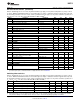
Symbol Parameter Conditions Min Typ Max Units
I
HBO
Total HB Operating Current f = 500 kHz 1.5 2.5 mA
I
HBS
HB to VSS Current, Quiescent HS = HB = 100V 0.1 8 µA
I
HBSO
HB to VSS Current, Operating f = 500 kHz 0.4 1.0 mA
INPUT PINS
V
IR
Input Voltage Threshold Rising Edge 1.89 2.06 2.18 V
V
IF
Input Voltage Threshold Falling Edge 1.48 1.66 1.76 V
V
IHYS
Input Voltage Hysteresis 400 mV
R
I
Input Pulldown Resistance 100 200 300 kΩ
UNDER VOLTAGE PROTECTION
V
DDR
VDD Rising Threshold 3.2 3.8 4.5 V
V
DDH
VDD Threshold Hysteresis 0.2 V
V
HBR
HB Rising Threshold 2.5 3.2 3.9 V
V
HBH
HB Threshold Hysteresis 0.2 V
BOOTSTRAP DIODE
V
DL
Low-Current Forward Voltage I
VDD-HB
= 100 µA 0.45 0.65 V
V
DH
High-Current Forward Voltage I
VDD-HB
= 100 mA 0.90 1.00 V
R
D
Dynamic Resistance I
VDD-HB
= 100 mA 1.85 3.60 Ω
HB-HS Clamp Regulation Voltage 4.7 5.2 5.45 V
LOW & HIGH SIDE GATE DRIVER
V
OL
Low-Level Output Voltage I
HOL
= I
LOL
= 100 mA 0.06 0.10 V
V
OH
High-Level Output Voltage I
HOH
= I
LOH
= 100 mA
0.21 0.31 V
V
OH
= VDD – LOH or V
OH
= HB – HOH
I
OHL
Peak Source Current HOH, LOH = 0V 1.2 A
I
OLL
Peak Sink Current HOL, LOL = 5V 5 A
I
OHLK
High-Level Output Leakage Current HOH, LOH = 0V 1.5 µA
I
OLLK
Low-Level Output Leakage Current HOL, LOL = 5V 1.5 µA
THERMAL RESISTANCE
θ
JA
Junction to Ambient
(2)
WSON-10 40 °C/W
12-bump DSBGA 80 °C/W
(2) Four layer board with Cu finished thickness 1.5/1/1/1.5 oz. Maximum die size used. 5x body length of Cu trace on PCB top. 50 x 50mm
ground and power planes embedded in PCB. See Application Note AN-1187 SNOA401.
Switching Characteristics
Limits in standard type are for T
J
= 25°C only; limits in boldface type apply over the junction temperature (T
J
) range of -40°C
to +125°C. Minimum and Maximum limits are ensured through test, design, or statistical correlation. Typical values represent
the most likely parametric norm at T
J
= 25°C, and are provided for reference purposes only. Unless otherwise specified, V
DD
=
V
HB
= 5V, V
SS
= V
HS
= 0V, No Load on LOL and LOH or HOL and HOH
(1)
.
Symbol Parameter Conditions Min Typ Max Units
t
LPHL
LO Turn-Off Propagation Delay LI Falling to LOL Falling 26.5 45.0 ns
t
LPLH
LO Turn-On Propagation Delay LI Rising to LOH Rising 28.0 45.0 ns
t
HPHL
HO Turn-Off Propagation Delay HI Falling to HOL Falling 26.5 45.0 ns
t
HPLH
HO Turn-On Propagation Delay HI Rising to HOH Rising 28.0 45.0 ns
t
MON
Delay Matching: LO on & HO off 1.5 8.0 ns
(1) Min and Max limits are 100% production tested at 25°C. Limits over the operating temperature range are ensured through correlation
using Statistical Quality Control (SQC) methods. Limits are used to calculate Average Outgoing Quality Level (AOQL).
Copyright © 2011–2013, Texas Instruments Incorporated Submit Documentation Feedback 5
Product Folder Links: LM5113