
Datasheet
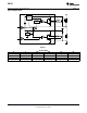
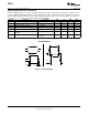
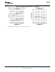

LI
HI
t
HPLH
t
LPLH
t
HPHL
t
LPHL
LO
HO
LI
HI
t
MOFF
t
MON
LO
HO
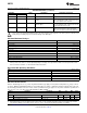
LM5113
SNVS725F –JUNE 2011–REVISED APRIL 2013
www.ti.com
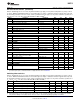
Switching Characteristics (continued)
Limits in standard type are for T
J
= 25°C only; limits in boldface type apply over the junction temperature (T
J
) range of -40°C
to +125°C. Minimum and Maximum limits are ensured through test, design, or statistical correlation. Typical values represent
the most likely parametric norm at T
J
= 25°C, and are provided for reference purposes only. Unless otherwise specified, V
DD
=
V
HB
= 5V, V
SS
= V
HS
= 0V, No Load on LOL and LOH or HOL and HOH
(1)
.
Symbol Parameter Conditions Min Typ Max Units
t
MOFF
Delay Matching: LO off & HO on 1.5 8.0 ns
t
HRC
HO Rise Time (0.5V - 4.5V) C
L
= 1000 pF 7.0 ns
t
LRC
LO Rise Time (0.5V – 4.5V) C
L
= 1000 pF 7.0 ns
t
HFC
HO Fall Time (0.5V - 4.5V) C
L
= 1000 pF 1.5 ns
t
LFC
LO Fall Time (0.5V - 4.5V) C
L
= 1000 pF 1.5 ns
t
PW
Minimum Input Pulse Width that Changes
10 ns
the Output
t
BS
Bootstrap Diode Reverse Recovery Time I
F
= 100mA,
40 ns
I
R
= 100mA
Timing Diagram
Figure 3. Timing Diagram
6 Submit Documentation Feedback Copyright © 2011–2013, Texas Instruments Incorporated
Product Folder Links: LM5113