
Datasheet
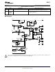


Main
Output
3.3V
V
BIAS
FB
AGND
COMP
Sync
V
CC
SS
HB
HO
HS
LO
PGND
V
OUT
CO
CS
RAMP
LM5115
Auxiliary
Output
2.0V
+12V
R
S
FEEDBACK
Main Converter
PWM Controller
INPUT
Phase Signal
LM5115
www.ti.com
SNVS343E –MARCH 2005–REVISED MARCH 2013
LM5115 Secondary Side Post Regulator / Synchronous Buck Controller
Check for Samples: LM5115
1
FEATURES
DESCRIPTION
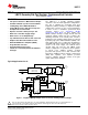
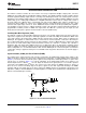
The LM5115 is a versatile switching regulator
2
• Self-Synchronization to Main Channel Output
controller. It has two main application configurations.
• Standalone DC/DC Synchronous Buck Mode
The first is utilizing the Secondary Side Post
• Leading Edge Pulse Width Modulation
Regulation (SSPR) technique to implement multiple
output power converters. In the second configuration,
• Voltage-Mode Control with Current Injection
it can be used as a standalone synchronous buck
and Input Line Feed-Forward
controller (Please see Standalone DC/DC
• Operates from AC or DC Input up to 75V
Synchronous Buck Mode for more details). The
• Wide 4.5V to 30V Bias Supply Range
SSPR technique develops a highly efficient and well
regulated auxiliary output from the secondary side
• Wide 0.75V to 13.5V Output Range.
switching waveform of an isolated power converter.
• Top and Bottom Gate Drivers Sink 2.5A Peak
Regulation of the auxiliary output voltage is achieved
• Adaptive Gate Driver Dead-Time Control
by leading edge pulse width modulation (PWM) of the
main channel duty cycle. Leading edge modulation is
• Wide Bandwidth Error Amplifier (4MHz)
compatible with either current mode or voltage mode
• Programmable Soft-Start
control of the main output. The LM5115 drives
• Thermal Shutdown Protection
external high side and low side NMOS power
switches configured as a synchronous buck regulator.
• TSSOP-16 or Thermally Enhanced WSON-16
A current sense amplifier provides overload
Packages
protection and operates over a wide common mode
input range. Additional features include a low dropout
(LDO) bias regulator, error amplifier, precision
reference, adaptive dead time control of the gate
signals and thermal shutdown.
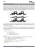
Typical Application Circuit
Figure 1. Simplified Multiple Output Power Converter Utilizing SSPR Technique
1
Please be aware that an important notice concerning availability, standard warranty, and use in critical applications of
Texas Instruments semiconductor products and disclaimers thereto appears at the end of this data sheet.
2All trademarks are the property of their respective owners.
PRODUCTION DATA information is current as of publication date.
Copyright © 2005–2013, Texas Instruments Incorporated
Products conform to specifications per the terms of the Texas
Instruments standard warranty. Production processing does not
necessarily include testing of all parameters.