LM5117, LM5117-Q1 www.ti.com SNVS698E – APRIL 2011 – REVISED MARCH 2013 Wide Input Range Synchronous Buck Controller with Analog Current Monitor Check for Samples: LM5117, LM5117-Q1 FEATURES DESCRIPTION • The LM5117 is a synchronous buck controller intended for step-down regulator applications from a high voltage or widely varying input supply. The control method is based upon current mode control utilizing an emulated current ramp.
LM5117, LM5117-Q1 SNVS698E – APRIL 2011 – REVISED MARCH 2013 www.ti.
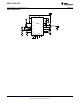
LM5117, LM5117-Q1 www.ti.com SNVS698E – APRIL 2011 – REVISED MARCH 2013 HO SS 4 17 SW RT 5 16 VCC AGND 6 15 LO VCCDIS 7 14 PGND FB 8 13 CSG COMP 9 12 CS CM 10 11 RAMP EP Figure 1.
LM5117, LM5117-Q1 SNVS698E – APRIL 2011 – REVISED MARCH 2013 www.ti.com PIN DESCRIPTIONS 4 HTSSOP Pin WQFN Pin Name Description 1 24 UVLO Under-voltage lockout programming pin. If the UVLO pin voltage is below 0.4V, the regulator is in the shutdown mode with all functions disabled. If the UVLO pin voltage is greater than 0.4V and less than 1.25V, the regulator is in standby mode with the VCC regulator operational, the SS pin grounded, and no switching at the HO and LO outputs.
LM5117, LM5117-Q1 www.ti.com SNVS698E – APRIL 2011 – REVISED MARCH 2013 PIN DESCRIPTIONS (continued) HTSSOP Pin WQFN Pin Name Description 17 NC No electrical contact. 21 NC No electrical contact. 23 NC No electrical contact. These devices have limited built-in ESD protection. The leads should be shorted together or the device placed in conductive foam during storage or handling to prevent electrostatic damage to the MOS gates. Absolute Maximum Ratings (1) VIN to AGND -0.
LM5117, LM5117-Q1 SNVS698E – APRIL 2011 – REVISED MARCH 2013 www.ti.com Electrical Characteristics Limits in standard type are for TJ = 25°C only; limits in boldface type apply over the junction temperature range of -40°C to +125°C. Typical values represent the most likely parametric norm at TJ = 25°C, and are provided for reference purposes only. Unless otherwise specified, the following conditions apply: VVIN = 48V, VVCCDIS = 0V, RT = 25kΩ, no load on LO & HO.
LM5117, LM5117-Q1 www.ti.com SNVS698E – APRIL 2011 – REVISED MARCH 2013 Electrical Characteristics (continued) Limits in standard type are for TJ = 25°C only; limits in boldface type apply over the junction temperature range of -40°C to +125°C. Typical values represent the most likely parametric norm at TJ = 25°C, and are provided for reference purposes only. Unless otherwise specified, the following conditions apply: VVIN = 48V, VVCCDIS = 0V, RT = 25kΩ, no load on LO & HO.
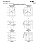
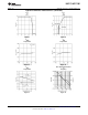
LM5117, LM5117-Q1 SNVS698E – APRIL 2011 – REVISED MARCH 2013 www.ti.com Typical Performance Characteristics 8 HO Peak Driver Current vs Output Voltage LO Peak Driver Current vs Output Voltage Figure 3. Figure 4. Driver Dead Time vs VVCC Driver Dead Time vs Temperature Figure 5. Figure 6. Forced HO Off-time vs Temperature Switching Frequency vs RT Figure 7. Figure 8.
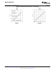
LM5117, LM5117-Q1 www.ti.com SNVS698E – APRIL 2011 – REVISED MARCH 2013 Typical Performance Characteristics (continued) VVCC vs IVCC VVCC vs VVIN Figure 9. Figure 10. VCS(TH) vs Temperature VREF vs Temperature Figure 11. Figure 12. VVCC vs Temperature Error Amp Gain and Phase vs Frequency Figure 13. Figure 14.
LM5117, LM5117-Q1 SNVS698E – APRIL 2011 – REVISED MARCH 2013 www.ti.com Typical Performance Characteristics (continued) 10 VCM vs IOUT VCM vs VCSG-CS Figure 15. Figure 16.
SYNC CSYNC CSS REF Copyright © 2011–2013, Texas Instruments Incorporated Product Folder Links: LM5117 LM5117-Q1 RES RES Current COMP FB SS RT + + ERR + AMP - + + - RESTART TIMER - 1.
LM5117, LM5117-Q1 SNVS698E – APRIL 2011 – REVISED MARCH 2013 www.ti.com FUNCTIONAL DESCRIPTION The LM5117 high voltage switching controller features all of the functions necessary to implement an efficient high voltage buck regulator that operates over a very wide input voltage range. This easy to use controller integrates high-side and low-side NMOS drivers. The regulator control method is based upon peak current mode control utilizing an emulated current ramp.
LM5117, LM5117-Q1 www.ti.com SNVS698E – APRIL 2011 – REVISED MARCH 2013 VOUT VCC LM5117 VCCDIS resistor divider is required when external VCC supplying voltage is smaller than 8.5V VCCDIS Figure 19. External VCC Supply for 6V< VOUT<14.5V For VOUT < 6V, a bias winding on the output inductor can be added to generate the external VCC supply voltage. VCC LM5117 VCCDIS VOUT SW VCCDIS resistor divider is required when external VCC supplying voltage is smaller than 8.5V Figure 20.
LM5117, LM5117-Q1 SNVS698E – APRIL 2011 – REVISED MARCH 2013 www.ti.com UVLO Hysteresis Current VIN UVLO Threshold RUV2 UVLO CFT RUV1 LM5117 UVLO Shutdown Threshold + + STANDBY SHUTDOWN Figure 22. UVLO Configuration The UVLO pin should not be left floating. An external UVLO set-point voltage divider from the VIN to AGND is used to set the minimum input operating voltage of the regulator. The divider must be designed such that the voltage at the UVLO pin is greater than 1.
LM5117, LM5117-Q1 www.ti.com SNVS698E – APRIL 2011 – REVISED MARCH 2013 Ramp Generator and Emulated Current Sense The ramp signal used in the pulse width modulator for traditional current mode control is typically derived directly from the high-side switch current. This switch current corresponds to the positive slope portion of the inductor current.
LM5117, LM5117-Q1 SNVS698E – APRIL 2011 – REVISED MARCH 2013 www.ti.com The selection of RRAMP and CRAMP can be simplified by adopting a K factor, which is defined as: K= LO RRAMP x CRAMP x RS x AS where • AS is the current sense amplifier gain which is normally 10 (4) By choosing 1 as the K factor, the regulator removes any error after one switching cycle and the design procedure is simplified. See Application Information section for detailed information.
LM5117, LM5117-Q1 www.ti.com SNVS698E – APRIL 2011 – REVISED MARCH 2013 The diode emulation feature is configured with the DEMB pin. To enable diode emulation, connect the DEMB pin to GND or leave the pin floating. If continuous conduction operation is desired, the DEMB pin should be tied to a voltage greater than 3V and may be connected to VCC. The LM5117 forces the regulator to operate in diode emulation mode when SS pin voltage is less than the internal 0.
LM5117, LM5117-Q1 SNVS698E – APRIL 2011 – REVISED MARCH 2013 VIN(MAX) x tON(MIN) VCS(TH) ILIM_PK = RS www.ti.com + [A] LO where • tON(MIN) is the minimum HO on-time (12) In most cases, especially if the output voltage is relatively high, it is recommended that a soft-saturating inductor such as a powder core device is used. If a sharp-saturating inductor is used, the inductor saturation level must be above ILIM_PK.
LM5117, LM5117-Q1 www.ti.com SNVS698E – APRIL 2011 – REVISED MARCH 2013 The RES pin can also be configured for latch-off mode current limiting or non-hiccup mode cycle-by-cycle current limiting. If the RES pin is tied to VCC or a voltage greater than the RES threshold at initial power-on, the restart timer is disabled and the regulator operates with non-hiccup mode cycle-by-cycle current limit.
LM5117, LM5117-Q1 SNVS698E – APRIL 2011 – REVISED MARCH 2013 www.ti.com Current Sense Amplifier Output LM5117 Current Monitor Amplifier CM CONDITIONER RCM AM = 2 40 k: CCM Figure 30. Current Monitor The average of CM output can be calculated by: VCM _ AVE = (IPEAK + IVALLEY )´ RS ´ A S [V ] (14) The current monitor output is only valid in continuous conduction operation. The current monitor has a limited bandwidth of approximately one tenth of fSW.
LM5117, LM5117-Q1 www.ti.com SNVS698E – APRIL 2011 – REVISED MARCH 2013 APPLICATION INFORMATION FEEDBACK COMPENSATION Open loop response of the regulator is defined as the product of modulator transfer function and feedback transfer function. When plotted on a dB scale, the open loop gain is shown as the sum of modulator gain and feedback gain.
LM5117, LM5117-Q1 SNVS698E – APRIL 2011 – REVISED MARCH 2013 www.ti.com fSW Zp_HF = K - 0.5 (18) The maximum achievable loop bandwidth, in fact, is limited by this sampled gain inductor pole. In traditional current mode control, the maximum achievable loop bandwidth varies with input voltage. With the LM5117’s unique slope compensation scheme, the sampled gain inductor pole is independent of changes to the input voltage.
LM5117, LM5117-Q1 www.ti.com SNVS698E – APRIL 2011 – REVISED MARCH 2013 Figure 33. dl1/dl0 vs K Factor The minimum value of K is 0.5. When K<0.5, the amplitude of dI1 is greater than the amplitude of dI0 and any initial perturbation results in sub-harmonic oscillation. If K=1, any initial perturbation will be removed in one switching cycle. This is known as one-cycle damping. When -1
LM5117, LM5117-Q1 SNVS698E – APRIL 2011 – REVISED MARCH 2013 www.ti.com Connect all of the low power ground connections (RUV1, RT, RFB1, CSS, CRES, CCM, CVIN, CRAMP) directly to the regulator AGND pin. Connect CVCC directly to the regulator PGND pin. Note that CVIN and CVCC must be as physically close as possible to the IC. AGND and PGND must be directly connected together through a top-side copper pattern connected to the exposed pad. Ensure no high current flows beneath the underside exposed pad.
LM5117, LM5117-Q1 www.ti.com SNVS698E – APRIL 2011 – REVISED MARCH 2013 The highest power dissipating components are the two power switches. Selecting NMOS switches with exposed pads aids the power dissipation of these devices. Table 1.
LM5117, LM5117-Q1 SNVS698E – APRIL 2011 – REVISED MARCH 2013 www.ti.com Table 1.
LM5117, LM5117-Q1 www.ti.com SNVS698E – APRIL 2011 – REVISED MARCH 2013 Design Example OPERATING CONDITIONS • • • • • • • Output Voltage VOUT = 12V Full Load Current IOUT = 9A Minimum Input Voltage VIN(MIN) = 15V Maximum Input Voltage VIN(MAX) = 55V Switching Frequency fSW = 230kHz Diode Emulation Yes External VCC Supply Yes TIMING RESISTOR RT Generally, higher frequency applications are smaller but have higher losses.
LM5117, LM5117-Q1 SNVS698E – APRIL 2011 – REVISED MARCH 2013 www.ti.com CURRENT SENSE RESISTOR RS The performance of the converter will vary depending on the K value. For this example, K=1 was chosen to control sub-harmonic oscillation and achieve one-cycle damping. The maximum output current capability (IOUT(MAX)) should be 20~50% higher than the required output current, to account for tolerances and ripple current. For this example, 130% of 9A was chosen.
LM5117, LM5117-Q1 www.ti.com SNVS698E – APRIL 2011 – REVISED MARCH 2013 UVLO DIVIDER RUV2, RUV1 AND CFT The desired startup voltage and the hysteresis are set by the voltage divider RUV1 and RUV2. Capacitor CFT provides filtering for the divider. For this design, the startup voltage was set to 14V, 1V below VIN(MIN). VHYS was set to 2V. The value of RUV1, RUV2 can be calculated from Equation 1 and Equation 2 as follows: RUV2 = 2V = 100 k: 20 µA (31) 1.25V x 100 k: RUV1 = = 9.8 k: 14V -1.
LM5117, LM5117-Q1 SNVS698E – APRIL 2011 – REVISED MARCH 2013 www.ti.com SNUBBER COMPONENTS RSNB AND CSNB A resistor-capacitor snubber network across the low-side NMOS device reduces ringing and spikes at the switching node. Excessive ringing and spikes can cause erratic operation and can couple noise to the output voltage. Selecting the values for the snubber is best accomplished through empirical methods. First, make sure the lead lengths for the snubber connections are very short.
LM5117, LM5117-Q1 www.ti.com SNVS698E – APRIL 2011 – REVISED MARCH 2013 In this example, seven 3.3μF ceramic capacitors were used. With ceramic capacitors, the input ripple voltage will be triangular. The input ripple voltage can be approximated as: IOUT 'VIN = 4 x fSW x CIN [V] (40) 9A = 0.42V 'VIN = 4 x 230 kHz x 3.3 PH x 7 (41) Capacitors connected in parallel should be evaluated for RMS current rating.
LM5117, LM5117-Q1 SNVS698E – APRIL 2011 – REVISED MARCH 2013 www.ti.com LOOP COMPENSATION COMPONENTS CCOMP, RCOMP and CHF RCOMP, CCOMP and CHF configure the error amplifier gain and phase characteristics to produce a stable voltage loop. For a quick start, follow the 4 steps listed below. For detailed information, see Application Information section.
LM5117, LM5117-Q1 www.ti.com SNVS698E – APRIL 2011 – REVISED MARCH 2013 Application Circuit Figure 35.
LM5117, LM5117-Q1 SNVS698E – APRIL 2011 – REVISED MARCH 2013 www.ti.com Example of Constant Current Regulator The LM5117 can be configured as a constant current regulator by using the current monitor feature (CM) as the feedback input. A voltage divider at the VCCDIS pin from VOUT to AGND can be used to protect against output over-voltage. When the VCCDIS pin voltage is greater than the VCCDIS threshold, the controller disables the VCC regulator and the VCC pin voltage decays.
LM5117, LM5117-Q1 www.ti.com SNVS698E – APRIL 2011 – REVISED MARCH 2013 VIN Current Control (CC) 100 k: VCC CIN UVLO VIN SW 10 k: 100: 15 k: RES DEMB VCC LM5117 100 k: PNP CVCC DHB HB RAMP CHB 1 nF 1500 pF HO 100 k: CM QH 68 PH VOUT CV Mode : 5V CC Mode: 2A SW LMV431 200 k: LO VCCDIS QL 80 PF CS 47 m: VOUT 3.24 k: CSG 34.8 k: 0.1 PF COMP FB RT SS AGND PGND 619: 22.1 k: 0.33 PF x2 Voltage Control (CV) Figure 37.
LM5117, LM5117-Q1 SNVS698E – APRIL 2011 – REVISED MARCH 2013 www.ti.com REVISION HISTORY Changes from Revision D (March 2013) to Revision E • 36 Page Changed layout of National Data Sheet to TI format ..........................................................................................................
PACKAGE OPTION ADDENDUM www.ti.
PACKAGE OPTION ADDENDUM www.ti.com 11-Apr-2013 Pb-Free (RoHS): TI's terms "Lead-Free" or "Pb-Free" mean semiconductor products that are compatible with the current RoHS requirements for all 6 substances, including the requirement that lead not exceed 0.1% by weight in homogeneous materials. Where designed to be soldered at high temperatures, TI Pb-Free products are suitable for use in specified lead-free processes.
PACKAGE MATERIALS INFORMATION www.ti.com 26-Mar-2013 TAPE AND REEL INFORMATION *All dimensions are nominal Device Package Package Pins Type Drawing SPQ Reel Reel A0 Diameter Width (mm) (mm) W1 (mm) B0 (mm) K0 (mm) P1 (mm) LM5117PMHE/NOPB HTSSOP PWP 20 250 178.0 16.4 LM5117PMHX/NOPB HTSSOP PWP 20 2500 330.0 LM5117PSQ/NOPB WQFN RTW 24 1000 178.
PACKAGE MATERIALS INFORMATION www.ti.com 26-Mar-2013 *All dimensions are nominal Device Package Type Package Drawing Pins SPQ Length (mm) Width (mm) Height (mm) LM5117PMHE/NOPB HTSSOP PWP LM5117PMHX/NOPB HTSSOP PWP 20 250 213.0 191.0 55.0 20 2500 367.0 367.0 38.0 LM5117PSQ/NOPB WQFN RTW 24 1000 210.0 185.0 35.0 LM5117PSQE/NOPB WQFN RTW 24 250 210.0 185.0 35.0 LM5117PSQX/NOPB WQFN RTW 24 4500 367.0 367.0 35.0 LM5117QPMHE/NOPB HTSSOP PWP 20 250 213.
MECHANICAL DATA PWP0020A MXA20A (Rev C) www.ti.
MECHANICAL DATA RTW0024A SQA24A (Rev B) www.ti.
IMPORTANT NOTICE Texas Instruments Incorporated and its subsidiaries (TI) reserve the right to make corrections, enhancements, improvements and other changes to its semiconductor products and services per JESD46, latest issue, and to discontinue any product or service per JESD48, latest issue. Buyers should obtain the latest relevant information before placing orders and should verify that such information is current and complete.