
Datasheet
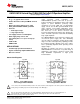
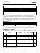
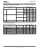
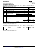
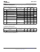
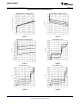
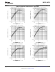
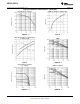
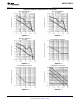
Table Of Contents
- FEATURES
- Applications
- DESCRIPTION
- Absolute Maximum Ratings
- Operating Ratings
- 5.0V DC Electrical Characteristics
- 5.0V AC Electrical Characteristics
- 2.7V DC Electrical Characteristics
- 2.7V AC Electrical Characteristics
- 24V DC Electrical Characteristics
- 24V AC Electrical Characteristics
- Typical Performance Characteristics
- Application Information
- Revision History
LM6152, LM6154
www.ti.com
SNOS752D –MAY 1999–REVISED MARCH 2013
LM6152/LM6154 Dual and Quad 75 MHz GBW Rail-to-Rail I/O Operational Amplifiers
Check for Samples: LM6152, LM6154
1
FEATURES
DESCRIPTION
Using patented circuit topologies, the
2
• At V
S
= 5V, typical unless noted.
LM6152/LM6154 provides new levels of speed vs.
• Greater than rail-to-rail input CMVR −0.25V to
power performance in applications where low voltage
5.25V
supplies or power limitations previously made
• Rail-to-rail output swing 0.01V to 4.99V
compromise necessary. With only 1.4 mA/amplifier
supply current, the 75 MHz gain bandwidth of this
• Wide gain-bandwidth 75 MHz @ 100 kHz
device supports new portable applications where
• Slew rate
higher power devices unacceptably drain battery life.
– Small signal 5 V/µs
The slew rate of the devices increases with
increasing input differential voltage, thus allowing the
– Large signal 45 V/µs
device to handle capacitive loads while maintaining
• Low supply current 1.4 mA/amplifier
large signal amplitude.
• Wide supply range 2.7V to 24V
The LM6152/LM6154 can be driven by voltages that
• Fast settling time of 1.1 µs for 2V step (to
exceed both power supply rails, thus eliminating
0.01%)
concerns about exceeding the common-mode voltage
• PSRR 91 dB
range. The rail-to-rail output swing capability provides
the maximum possible dynamic range at the output.
• CMRR 84 dB
This is particularly important when operating on low
supply voltages.
APPLICATIONS
Operating on supplies from 2.7V to over 24V, the
• Portable high speed instrumentation
LM6152/LM6154 is excellent for a very wide range of
• Signal conditioning amplifier/ADC buffers
applications, from battery operated systems with
large bandwidth requirements to high speed
• Barcode scanners
instrumentation.
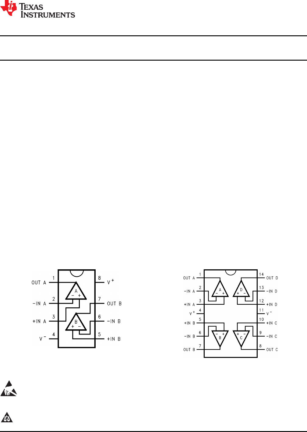
Connection Diagrams
Top View Top View
Figure 1. 8-Pin SOIC Package Figure 2. 14-Pin SOIC Package
See Package Number D0008A See Package Number D0014A
These devices have limited built-in ESD protection. The leads should be shorted together or the device placed in conductive foam
during storage or handling to prevent electrostatic damage to the MOS gates.
1
Please be aware that an important notice concerning availability, standard warranty, and use in critical applications of
Texas Instruments semiconductor products and disclaimers thereto appears at the end of this data sheet.
2All trademarks are the property of their respective owners.
PRODUCTION DATA information is current as of publication date.
Copyright © 1999–2013, Texas Instruments Incorporated
Products conform to specifications per the terms of the Texas
Instruments standard warranty. Production processing does not
necessarily include testing of all parameters.