
Datasheet

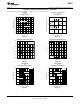

1
10
1k
10k 100k
FREQUENCY (Hz)
1
10
100
1000
100
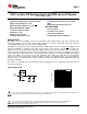
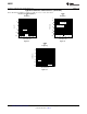
VOLTAGE NOISE
(nV/
Hz)
V
S
= 5V, 24V
+
-
VCO
INPUT
CHARGE
PUMP
OUTPUT
V
S_PLL
2
LM6211
www.ti.com
SNOSAH2C –FEBRUARY 2006–REVISED MARCH 2013
LM6211 Low Noise, RRO Operational Amplifier with CMOS Input and 24V Operation
Check for Samples: LM6211
1
FEATURES
• Temperature Range -40°C to 125°C
2
(Typical 24V Supply Unless Otherwise Noted)
• Total Harmonic Distortion 0.01% @ 1 kHz,
600Ω
• Supply Voltage Range 5V to 24V
• Output Short Circuit Current 25 mA
• Input Referred Voltage Noise 5.5 nV/√Hz
APPLICATIONS
• Unity Gain Bandwidth 20 MHz
• PLL Loop Filters
• 1/f Corner Frequency 400 Hz
• Low Noise Active Filters
• Slew Rate 5.6 V/μs
• Strain Gauge Amplifiers
• Supply Current 1.05 mA
• Low Noise Microphone Amplifiers
• Low Input Capacitance 5.5 pF
DESCRIPTION
The LM6211 is a wide bandwidth, low noise op amp with a wide supply voltage range and a low input bias
current. The LM6211 operates with a single supply voltage of 5V to 24V, is unity gain stable, has a ground-
sensing CMOS input stage, and offers rail-to-rail output swing.
The LM6211 is designed to provide optimal performance in high voltage, low noise systems. The LM6211 has a
unity gain bandwidth of 20 MHz and an input referred voltage noise density of 5.5 nV/√Hz at 10 kHz. The
LM6211 achieves these specifications with a low supply current of only 1 mA. The LM6211 has a low input bias
current of 2.3 pA, an output short circuit current of 25 mA and a slew rate of 5.6 V/us. The LM6211 also features
a low common-mode input capacitance of 5.5 pF which makes it ideal for use in wide bandwidth and high gain
circuits. The LM6211 is well suited for low noise applications that require an op amp with very low input bias
currents and a large output voltage swing, like active loop-filters for wide-band PLLs. A low total harmonic
distortion, 0.01% at 1 kHz with loads as high as 600Ω, also makes the LM6211 ideal for high fidelity audio and
microphone amplifiers.
The LM6211 is available in the small SOT-23 package, allowing the user to implement ultra-small and cost
effective board layouts.
Typical Application
These devices have limited built-in ESD protection. The leads should be shorted together or the device placed in conductive foam
during storage or handling to prevent electrostatic damage to the MOS gates.
1
Please be aware that an important notice concerning availability, standard warranty, and use in critical applications of
Texas Instruments semiconductor products and disclaimers thereto appears at the end of this data sheet.
2All trademarks are the property of their respective owners.
PRODUCTION DATA information is current as of publication date.
Copyright © 2006–2013, Texas Instruments Incorporated
Products conform to specifications per the terms of the Texas
Instruments standard warranty. Production processing does not
necessarily include testing of all parameters.