
Datasheet

LM628, LM629
SNVS781C –JUNE 1999–REVISED MARCH 2013
www.ti.com
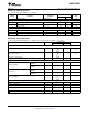
AC Electrical Characteristics (continued)
(V
DD
and T
A
per Operating Ratings; f
CLK
= 6 MHz; C
LOAD
= 50 pF; Input Test Signal t
r
= t
f
= 10 ns)
Tested Limits
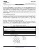
Timing Interval T# Units
Min Max
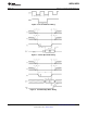
COMMAND BYTE WRITE TIMING (See Figure 6)
Chip-Select Setup/Hold Time T7 0 ns
Port-Select Setup Time T8 30 ns
Port-Select Hold Time T9 30 ns
Busy Bit Delay T13 See
(1)
ns
WR Pulse Width T14 100 ns
Write Data Setup Time T15 50 ns
Write Data Hold Time T16 120 ns
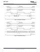
DATA WORD READ TIMING (See Figure 7)
Chip-Select Setup/Hold Time T7 0 ns
Port-Select Setup Time T8 30 ns
Port-Select Hold Time T9 30 ns
Read Data Access Time T10 180 ns
Read Data Hold Time T11 0 ns
RD High to Hi-Z Time T12 180 ns
Busy Bit Delay T13 See
(1)
ns
Read Recovery Time T17 120 ns
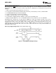
DATA WORD WRITE TIMING (See Figure 8)
Chip-Select Setup/Hold Time T7 0 ns
Port-Select Setup Time T8 30 ns
Port-Select Hold Time T9 30 ns
Busy Bit Delay T13 See
(1)
ns
WR Pulse Width T14 100 ns
Write Data Setup Time T15 50 ns
Write Data Hold Time T16 120 ns
Write Recovery Time T18 120 ns
(1) In order to read the busy bit, the status byte must first be read. The time required to read the busy bit far exceeds the time the chip
requires to set the busy bit. It is, therefore, impossible to test actual busy bit delay. The busy bit is ensured to be valid as soon as the
user is able to read it.
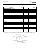
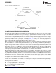
Figure 3. Quadrature Encoder Input Timing
4 Submit Documentation Feedback Copyright © 1999–2013, Texas Instruments Incorporated
Product Folder Links: LM628 LM629