
Datasheet

LM628, LM629
www.ti.com
SNVS781C –JUNE 1999–REVISED MARCH 2013
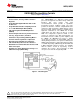
Pinout Description
(See Connection Diagrams) Pin numbers for the 24-pin surface mount package are indicated in parentheses.
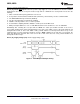
Pin 1 (17), Index (IN) Input: Receives optional index pulse from the encoder. Must be tied high if not used. The
index position is read when Pins 1, 2, and 3 are low.
Pins 2 and 3 (18 and 19), Encoder Signal (A, B) Inputs: Receive the two-phase quadrature signals provided
by the incremental encoder. When the motor is rotating in the positive (“forward”) direction, the signal at Pin 2
leads the signal at Pin 3 by 90 degrees. Note that the signals at Pins 2 and 3 must remain at each encoder state
(See Figure 10) for a minimum of 8 clock periods in order to be recognized. Because of a four-to-one resolution
advantage gained by the method of decoding the quadrature encoder signals, this corresponds to a maximum
encoder-state capture rate of 1.0 MHz (f
CLK
= 8.0 MHz) or 750 kHz (f
CLK
= 6.0 MHz). For other clock frequencies
the encoder signals must also remain at each state a minimum of 8 clock periods.
Pins 4 to 11 (20 to 24 and 2 to 4), Host I/O Port (D0 to D7): Bi-directional data port which connects to host
computer/processor. Used for writing commands and data to the LM628, and for reading the status byte and data
from the LM628, as controlled by CS (Pin 12), PS (Pin 16), RD (Pin 13), and WR (Pin 15).
Pin 12 (5), Chip Select (CS ) Input: Used to select the LM628 for writing and reading operations.
Pin 13 (6), Read (RD ) Input: Used to read status and data.
Pin 14 (7), Ground (GND): Power-supply return pin.
Pin 15 (8), Write (WR ) Input: Used to write commands and data.
Pin 16 (9), Port Select (PS ) Input: Used to select command or data port. Selects command port when low,
data port when high. The following modes are controlled by Pin 16:
1. Commands are written to the command port (Pin 16 low),
2. Status byte is read from command port (Pin 16 low), and
3. Data is written and read via the data port (Pin 16 high).
Pin 17 (10), Host Interrupt (HI) Output: This active-high signal alerts the host (via a host interrupt service
routine) that an interrupt condition has occurred.
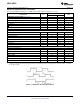
Pins 18 to 25, DAC Port (DAC0 to DAC7): Output port which is used in three different modes:
1. LM628 (8-bit output mode): Outputs latched data to the DAC. The MSB is Pin 18 and the LSB is Pin 25.
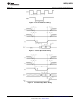
2. LM628 (12-bit output mode): Outputs two, multiplexed 6-bit words. The less-significant word is output first.
The MSB is on Pin 18 and the LSB is on Pin 23. Pin 24 is used to demultiplex the words; Pin 24 is low for
the less-significant word. The positive-going edge of the signal on Pin 25 is used to strobe the output data.
Figure 9 shows the timing of the multiplexed signals.
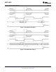
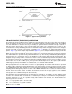
3. LM629 (sign/magnitude outputs): Outputs a PWM sign signal on Pin 18 (11 for surface mount), and a PWM
magnitude signal on Pin 19 (13 for surface mount). Pins 20 to 25 are not used in the LM629. Figure 12
shows the PWM output signal format.
Pin 26 (14), Clock (CLK) Input: Receives system clock.
Copyright © 1999–2013, Texas Instruments Incorporated Submit Documentation Feedback 7
Product Folder Links: LM628 LM629