
Datasheet

LM628, LM629
SNVS781C –JUNE 1999–REVISED MARCH 2013
www.ti.com
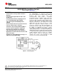
Pin 27 (15), Reset (RST) Input: Active-low, positive-edge triggered, resets the LM628 to the internal conditions
shown below. Note that the reset pulse must be logic low for a minimum of 8 clock periods. Reset does the
following:
1. Filter coefficient and trajectory parameters are zeroed.
2. Sets position error threshold to maximum value (7FFF hex), and effectively executes command LPEI.
3. The SBPA/SBPR interrupt is masked (disabled).
4. The five other interrupts are unmasked (enabled).
5. Initializes current position to zero, or “home” position.
6. Sets derivative sampling interval to 2048/f
CLK
or 256 μs for an 8.0 MHz clock.
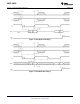
7. DAC port outputs 800 hex to “zero” a 12-bit DAC and then reverts to 80 hex to “zero” an 8-bit DAC.
Immediately after releasing the reset pin from the LM628, the status port should read “00”. If the reset is
successfully completed, the status word will change to hex “84” or “C4” within 1.5 ms. If the status word has not
changed from hex “00” to “84” or “C4” within 1.5 ms, perform another reset and repeat the above steps. To be
certain that the reset was properly performed, execute a RSTI command. If the chip has reset properly, the
status byte will change from hex “84” or “C4” to hex “80” or “C0”. If this does not occur, perform another reset
and repeat the above steps.
Pin 28 (16), Supply Voltage (V
DD
): Power supply voltage (+5V).
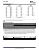
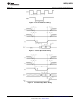
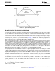
Figure 9. 12-Bit Multiplexed Output Timing
8 Submit Documentation Feedback Copyright © 1999–2013, Texas Instruments Incorporated
Product Folder Links: LM628 LM629