LM7121 LM7121 235 MHz Tiny Low Power Voltage Feedback Amplifier Literature Number: SNOS750
LM7121 235 MHz Tiny Low Power Voltage Feedback Amplifier General Description Features The LM7121 is a high performance operational amplifier which addresses the increasing AC performance needs of video and imaging applications, and the size and power constraints of portable applications. The LM7121 can operate over a wide dynamic range of supply voltages, from 5V (single supply) up to ± 15V (see the Application Information section for more details).
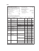
Absolute Maximum Ratings (Note 1) Storage Temperature Range Junction Temperature (Note 4) If Military/Aerospace specified devices are required, please contact the National Semiconductor Sales Office/ Distributors for availability and specifications. ESD Tolerance (Note 2) Differential Input Voltage (Note 7) Voltage at Input/Output Pin Supply Voltage (V+–V−) Output Short Circuit to Ground (Note 3) Lead Temperature (soldering, 10 sec) −65˚C to +150˚C 150˚C Operating Ratings (Note 1) 2000V ± 2V (V+)−1.
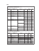
± 15V DC Electrical Characteristics (Continued) Unless otherwise specified, all limits guaranteed for TJ = 25˚C, V+ = +15V, V− = −15V, VCM = VO = 0V and RL > 1 MΩ. Boldface limits apply at the temperature extremes. Symbol Parameter Conditions Typ (Note 5) LM7121I Units Limit (Note 6) Supply Current IS 5.3 6.6 mA 7.5 max ± 15V AC Electrical Characteristics Unless otherwise specified, all limits guaranteed for TJ = 25˚C, V+ = 15V, V− = −15V, VCM = VO = 0V and RL > 1 MΩ.
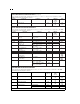
± 5V DC Electrical Characteristics (Continued) Unless otherwise specified, all limits guaranteed for TJ = 25˚C, V+ = 5V, V− = −5V, VCM = VO = 0V and RL > 1 MΩ. Boldface limits apply at the temperature extremes. Symbol Parameter Conditions Typ (Note 5) LM7121I Units Limit (Note 6) CIN Input Capacitance Common Mode 2.
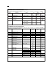
± 5V AC Electrical Characteristics (Continued) Unless otherwise specified, all limits guaranteed for TJ = 25˚C, V+ = 5V, V− = −5V, VCM = VO = 0V and RL > 1 MΩ. Boldface limits apply at the temperature extremes. Symbol Parameter Conditions Typ (Note 5) LM7121I Units Limit (Note 6) φD Differential Phase en Input-Referred AV = +2, RL = 150Ω f = 10 kHz 0.65 Deg 17 Voltage Noise Input-Referred in f = 10 kHz 2 Current Noise T.H.D.
+5V AC Electrical Characteristics Unless otherwise specified, all limits guaranteed for TJ = 25˚C, V+ = +5V, V− = 0V, VCM = VO = V+/2 and RL > 1 MΩ. Boldface limits apply at the temperature extremes. Symbol Parameter Conditions Typ (Note 5) LM7121I Units Limit (Note 6) SR AV = +2, RL = 1 kΩ to V+/2, VO = 1.8 VPP Slew Rate (Note 8) Rise and Fall Time RL = 1k, to V+/2 RL = 1k to V+/2 RL = 100Ω to V+/2, AV = +1 RL = 100Ω to V+/2, AV = +2 AV = +2, RL = 100Ω, (Note 10) VO = 0.
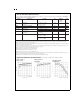
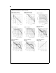
Typical Performance Characteristics TA = 25˚C, RL = 1 MΩ.
Typical Performance Characteristics Output Voltage vs Output Current (ISOURCE, VS = +5V) TA = 25˚C, RL = 1 MΩ. unless otherwise specified (Continued) Output Voltage vs Output Current (ISINK, VS = +5V) DS012348-88 DS012348-5 DS012348-4 Open Loop Frequency Response DS012348-89 www.national.
Typical Performance Characteristics GBWP @ 10 MHz vs Supply Voltage TA = 25˚C, RL = 1 MΩ.
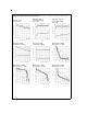
Typical Performance Characteristics TA = 25˚C, RL = 1 MΩ. unless otherwise specified (Continued) Slew Rate vs Load Capacitance Slew Rate vs Input Voltage Large Signal Pulse Response, AV = −1, VS = ± 15V DS012348-35 DS012348-33 Large Signal Pulse Response, AV = −1, VS = ± 5V DS012348-34 Large Signal Pulse Response, AV = −1, VS = +5V DS012348-37 DS012348-36 Large Signal Pulse Response, AV = +1, VS = ± 5V DS012348-38 Large Signal Pulse Response, AV = +1, VS = +5V DS012348-40 DS012348-39 www.
Typical Performance Characteristics Large Signal Pulse Response, AV = +2, VS = ± 5V TA = 25˚C, RL = 1 MΩ.
Typical Performance Characteristics Small Signal Pulse Response, AV = +2, VS = ± 5V, RL = 100Ω TA = 25˚C, RL = 1 MΩ.
Typical Performance Characteristics Closed Loop Frequency Response vs Capacitive Load (AV = +1, VS = ± 5V) TA = 25˚C, RL = 1 MΩ.
Typical Performance Characteristics TA = 25˚C, RL = 1 MΩ. unless otherwise specified (Continued) Undistorted Output Swing vs Frequency Total Power Dissipation vs Ambient Temperature DS012348-86 DS012348-65 Application Information In determining maximum operable temperature of the device, make sure the total power dissipation of the device is considered; this includes the power dissipated in the device with a load connected to the output as well as the nominal dissipation of the op amp.
Application Information (Continued) DS012348-93 FIGURE 3. Waveform across a 100Ω Load Color Video on Twisted Pairs Using Single Supply The circuit shown in Figure 4 can be used to drive in excess of 25 meters length of twisted pair cable with no loss of resolution or picture definition when driving a NTSC monitor at the load end. It is very important to keep the lead lengths to a minimum and to provide a low impedance current path by using a ground-plane on the board.
Application Information (Continued) DS012348-94 Note: Pin numbers shown are for SO-8 package. *Input termination of NTSC monitor. FIGURE 4. Single Supply Differential Twister Pair Cable Transmitter/Receiver 8.5V ≤ VCC ≤ 30V Even though the transmission line is not terminated in its nominal characteristic impedance of about 600Ω, the resulting reflection at the load is only about 5% of the total signal and in most cases can be neglected.
Application Information (Continued) DS012348-95 FIGURE 5. Step Response to a 1 VPP Input Signal Measured across the 75Ω Load DS012348-98 (a) AV = −1 DS012348-99 CC = 2 pF for RL = 100Ω CC = Open for RL = Open (b) AV = +2 DS012348-A0 (c) AV = +2, Capacitive Load DS012348-A1 RF = 0Ω, CC = Open for VS < 6V RF = 510Ω, CC = 3 pF for VS ≥ 6V (d) AV = +1 DS012348-A2 (e) AV = +1, VS = +5V, Single Supply Operation FIGURE 6. Application Test Circuits 17 www.national.
Physical Dimensions inches (millimeters) unless otherwise noted 8-Lead (0.150" Wide) Small Outline Package, JEDEC Order Number LM7121IM or LM7121IMX NS Package Number M08A www.national.
LM7121 235 MHz Tiny Low Power Voltage Feedback Amplifier Physical Dimensions inches (millimeters) unless otherwise noted (Continued) 5-Lead Molded SOT23-5 Order Number LM7121IM5 or LM7121IM5X NS Package Number MA05A LIFE SUPPORT POLICY NATIONAL’S PRODUCTS ARE NOT AUTHORIZED FOR USE AS CRITICAL COMPONENTS IN LIFE SUPPORT DEVICES OR SYSTEMS WITHOUT THE EXPRESS WRITTEN APPROVAL OF THE PRESIDENT AND GENERAL COUNSEL OF NATIONAL SEMICONDUCTOR CORPORATION. As used herein: 1.
IMPORTANT NOTICE Texas Instruments Incorporated and its subsidiaries (TI) reserve the right to make corrections, modifications, enhancements, improvements, and other changes to its products and services at any time and to discontinue any product or service without notice. Customers should obtain the latest relevant information before placing orders and should verify that such information is current and complete.