
Datasheet


V
DET+
+2.0V
OPEN DRAIN OUTPUT
CMOS OUTPUT
1V
GND
5.0V
2.5V
GND
50%
t
D1
t
D2
t
D1
t
D2
GND
GND
1V
V
DET+
+2.0V
V
DET+
+2.0V
V
DET+
+2.0V
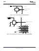
2
INPUT VOLTAGE,
PIN 2
RESET OUTPUT
VOLTAGE, PIN 1
LM8365
SNVS233B –MARCH 2003–REVISED APRIL 2013
www.ti.com
APPLICATION NOTES
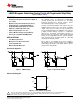
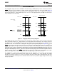
The propagation delay time for the LM8365 is measured using a 470kΩ pull-up resistor connected to from the
RESET output pin to 5V in addition to a 10pF capacitive load connected from the same pin to GND. Figure 15
shows the timing diagram for the measurement for the propagation delay. V
DET+
is equal to the sum of the
detector threshold, V
DET−
, and the built in hysteresis, V
HYS
. t
D1
is the propagation time from High-to-Low and t
D2
is
the propagation from Low-to-High.
Figure 15. Propagation Delay Timing Diagrams
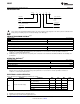
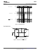
The LM8365 ultra-low current voltage detector was designed to monitor voltages and to provide an indication
when the monitored voltage, V
IN
, dropped below a precisely trimmed threshold voltage. The voltage detector of
the LM8365 drives a time delay generator that may be programmed for fixed lengths of time depending on the
application needs. This characteristic is displayed in the typical operating timing diagram in Figure 16. V
IN
is the
voltage that is being monitored and as it decreases passed the precisely trimmed threshold V
DET−
the Active Low
RESET output drops to a Logic Low state and the C
D
pin drops to 0V. During this state the external capacitor
connected to the C
D
pin is immediately discharged by an internal N-Channel MOSFET. When V
IN
increases
above the threshold V
DET+
(V
DET−
+ V
HYS
) the capacitor connected to the C
D
pin starts to charge up to V
IN
through an internal pull-up resistor R
D
. Once the capacitor has charged up past the internal Delay Pin Threshold,
which is typically 0.675 V
IN
, the RESET output will revert back to it's original state. The LM8365 has built-in
hysteresis to help prevent erratic reset operation when the input voltage crosses the threshold.
The LM8365 has a wide variety of applications that can take advantage of it's precision and low current
consumption to monitor Input voltages even though it was designed as a reset controller in portable
microprocessor based systems. It is a very cost effective and space saving device that will protect your more
expensive investments of microprocessors and other devices that need a specified supply voltage and time delay
for proper operation.
6 Submit Documentation Feedback Copyright © 2003–2013, Texas Instruments Incorporated
Product Folder Links: LM8365