LM83 LM83 Triple-Diode Input and Local Digital Temperature Sensor with Two-Wire Interface Literature Number: SNIS111A
LM83 Triple-Diode Input and Local Digital Temperature Sensor with Two-Wire Interface General Description The LM83 is a digital temperature sensor with a 2 wire serial interface that senses the voltage and thus the temperature of three remote diodes using a Delta-Sigma analog-to-digital converter with a digital over-temperature detector. The LM83 accurately senses its own temperature as well as the temperature of three external devices, such as Pentium II ® Processors or diode connected 2N3904s.
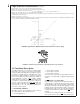
LM83 Connection Diagram Ordering Information QSOP-16 Order Number NS Package Number Transport Media LM83CIMQA MQA16A (QSOP-16) 95 Units in Rail LM83CIMQAX MQA16A (QSOP-16) 2500 Units on Tape and Reel DS101058-2 TOP VIEW Typical Application DS101058-3 Pin Description Label Pin # D1+, D2+, D3+ 1, 3, 5 VCC 2 www.national.com Function Typical Connection Diode Current Source To Diode Anode.
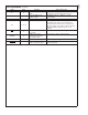
Label LM83 Pin Description (Continued) Pin # Function Typical Connection D− 4 Diode Return Current Sink To all Diode Junction Cathodes using a star connection to pin. Must float when not used. ADD0–ADD1 10, 6 User-Set SMBus (I2C) Address Inputs Ground (Low, “0”), VCC (High, “1”) or open (“TRI-LEVEL”) GND 7, 8 Power Supply Ground Ground Manufacturing test pins. Left floating.
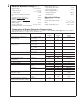
LM83 Absolute Maximum Ratings (Note 1) Supply Voltage Voltage at Any Pin QSOP Package (Note 3) Vapor Phase (60 seconds) Infrared (15 seconds) ESD Susceptibility (Note 4) Human Body Model Machine Model −0.3 V to 6.0 V −0.3 V to (VCC + 0.3 V) ± 1 mA D− Input Current Input Current at All Other Pins (Note 2) 5 mA Package Input Current (Note 2) 20 mA SMBData, T_CRIT_A, INT Output Sink Current 10 mA SMBCLK, SMBData, T_CRIT_A, INT Output Voltage 6.
DIGITAL DC CHARACTERISTICS Unless otherwise noted, these specifications apply for VCC =+3.0 to 3.6 Vdc. Boldface limits apply for TA = TJ = TMIN to TMAX; all other limits TA = TJ =+25˚C, unless otherwise noted. Symbol Parameter Conditions Typical Limits Units (Note 6) (Note 7) (Limit) SMBData, SMBCLK VIN(1) Logical “1” Input Voltage 2.1 V (min) VIN(0) Logical “0”Input Voltage 0.
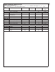
LM83 Logic Electrical Characteristics (Continued) SMBus DIGITAL SWITCHING CHARACTERISTICS Unless otherwise noted, these specifications apply for VCC =+3.0 Vdc to +3.6 Vdc, CL (load capacitance) on output lines = 80 pF. Boldface limits apply for TA = TJ = TMIN to TMAX; all other limits TA = TJ = +25˚C, unless otherwise noted. The switching characteristics of the LM83 fully meet or exceed the published specifications of the SMBus or I2C bus.
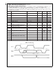
LM83 Logic Electrical Characteristics (Continued) SMBus TIMEOUT DS101058-7 See drawing DS10105807 Note 1: Absolute Maximum Ratings indicate limits beyond which damage to the device may occur. DC and AC electrical specifications do not apply when operating the device beyond its rated operating conditions. Note 2: When the input voltage (VI) at any pin exceeds the power supplies (VI < GND or VI > VCC), the current at that pin should be limited to 5 mA.
LM83 Logic Electrical Characteristics (Continued) Note 6: Typicals are at TA = 25˚C and represent most likely parametric norm. Note 7: Limits are guaranteed to National’s AOQL (Average Outgoing Quality Level). Note 8: The Temperature Error will vary less than ± 1.0 ˚C for a variation in VCC of 3 V to 3.6 V from the nominal of 3.3 V. Note 9: Quiescent current will not increase substantially with an active SMBus.
Local and remote temperature diodes are sampled in sequence by the A/D converter. The T_CRIT_A output and the Status Register flags are updated at the completion of a conversion. T_CRIT_A and the Status Register flags are reset only after the Status Register is read and if a temperature conversion is below the T_CRIT setpoint, as shown in Figure 6. Figure 7 shows a simplified logic diagram of the T_CRIT_A and related circuitry.
LM83 1.0 Functional Description 3. Diode 1, Diode 2, and Diode 3 Remote Temperature set to 0˚C until the LM83 senses a diode present between the D+ and D− input pins. 4. Status Registers 1 and 2 set to 00h. 5. Configuration Register set to 00h; INT enabled and all T_CRIT setpoints enabled to activate T_CRIT_A. 6. 1.
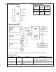
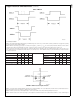
LM83 1.0 Functional Description (Continued) 1.9 COMMUNICATING with the LM83 DS101058-9 There are 19 data registers in the LM83, selected by the Command Register. At power-up the Command Register is set to “00”, the location for the Read Local Temperature Register. The Command Register latches the last location it was set to. Reading the Status Register resets T_CRIT_A and INT, so long as a temperature comparison does not signal a fault (see Sections 1.2 and 1.3).
LM83 1.0 Functional Description (Continued) the serial interface logic if either of the SMBData or SMBCLK lines are held low between 25 ms and 40 ms. TIMEOUT allows a clean recovery in cases where the master may be reset while the LM83 is transmitting a low bit thus preventing possible bus lock up. Whenever the LM83 sees the start condition its serial interface will reset to the beginning of the communication, thus the LM83 will expect to see an address byte next.
LM83 1.0 Functional Description (Continued) 2.0 LM83 REGISTERS 2.1 COMMAND REGISTER Selects which registers will be read from or written to. Data for this register should be transmitted during the Command Byte of the SMBus write communication.
LM83 1.0 Functional Description Command Select Address (Continued) Power On Default State < P7:P0 > hex < D7:D0 > binary Register Name Register Function < D7:D0 > decimal 5Ch-6Fh and F0h-FDh Reserved for Future Use FEh 0000 0001 1 FFh RMID Read Manufacturers ID RSR Read Stepping or Die Revision Code 2.
LM83 1.0 Functional Description (Continued) D5: T_CRIT mask for Diode 1, when set to 1 a Diode 1 temperature reading that exceeds T_CRIT setpoint will not activate the T_CRIT_A pin. D4: T_CRIT mask for Diode 2, when set to 1 a Diode 2 temperature reading that exceeds T_CRIT setpoint will not activate the T_CRIT_A pin. D3: T_CRIT mask for Diode 3, when set to 1 a Diode 3 temperature reading that exceeds T_CRIT setpoint will not activate the T_CRIT_A pin.
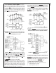
LM83 3.0 SMBus Timing Diagrams DS101058-10 (a) Serial Bus Write to the internal Command Register followed by a the Data Byte DS101058-11 (b) Serial Bus Write to the internal Command Register DS101058-12 (c) Serial Bus Read from a Register with the internal Command Register preset to desired value. FIGURE 8. Serial Bus Timing Diagrams www.national.
LM83 4.0 Application Hints The LM83 can be applied easily in the same way as other integrated-circuit temperature sensors, and its remote diode sensing capability allows it to be used in new ways as well. It can be soldered to a printed circuit board, and because the path of best thermal conductivity is between the die and the pins, its temperature will effectively be that of the printed circuit board lands and traces soldered to the LM83’s pins.
LM83 4.0 Application Hints 6. (Continued) Avoid running diode traces close to or parallel to high speed digital and bus lines. Diode traces should be kept at least 2cm. apart from the high speed digital traces. 7. If it is necessary to cross high speed digital traces, the diode traces and the high speed digital traces should cross at a 90 degree angle. 8. The ideal place to connect the LM83’s GND pin is as close as possible to the Processors GND associated with the sense diode.
LM83 4.0 Typical Applications (Continued) DS101058-23 Any two or three D+ inputs can be connected in parallel to increase the number of High temperature setpoints for a particular temperature reading. If all three D+ inputs are tied as shown here, D1+, D2+ and D3+ temperature readings will be identical, unless affected by PCB D+ trace resistance differences. FIGURE 12.
LM83 Triple-Diode Input and Local Digital Temperature Sensor with Two-Wire Interface Physical Dimensions inches (millimeters) unless otherwise noted 16-Lead QSOP Package Order Number LM83CIMQA or LM83CIMQAX NS Package Number MQA16 LIFE SUPPORT POLICY NATIONAL’S PRODUCTS ARE NOT AUTHORIZED FOR USE AS CRITICAL COMPONENTS IN LIFE SUPPORT DEVICES OR SYSTEMS WITHOUT THE EXPRESS WRITTEN APPROVAL OF THE PRESIDENT AND GENERAL COUNSEL OF NATIONAL SEMICONDUCTOR CORPORATION. As used herein: 1.
IMPORTANT NOTICE Texas Instruments Incorporated and its subsidiaries (TI) reserve the right to make corrections, modifications, enhancements, improvements, and other changes to its products and services at any time and to discontinue any product or service without notice. Customers should obtain the latest relevant information before placing orders and should verify that such information is current and complete.