
Datasheet
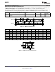
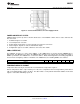

SNP
V+
GND
D1
D2
D3
D5
D4
R1
ESD
Clamp
D6
D7
I/O
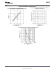
V
IH
V
IL
SMBCLK
P S
V
IH
V
IL
SMBDAT
t
BUF
t
HD;STA
t
LOW
t
R
t
HD;DAT
t
HIGH
t
F
t
SU;DAT
t
SU;STA
t
SU;STO
P
LM95221
SNIS134B –MAY 2004–REVISED MARCH 2013
www.ti.com
SMBus DIGITAL SWITCHING CHARACTERISTICS
Unless otherwise noted, these specifications apply for V
DD
=+3.0 Vdc to +3.6 Vdc, C
L
(load capacitance) on output lines = 80
pF. Boldface limits apply for T
A
= T
J
= T
MIN
to T
MAX
; all other limits T
A
= T
J
= +25°C, unless otherwise noted.
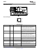
The switching characteristics of the LM95221 fully meet or exceed the published specifications of the SMBus version 2.0. The
following parameters are the timing relationships between SMBCLK and SMBDAT signals related to the LM95221. They
adhere to but are not necessarily the SMBus bus specifications.
Symbol Parameter Conditions Typical
(1)
Limits
(2)
Units
(Limit)
t
BUF
SMBus Free Time Between Stop and Start 1.3 µs (min)
Conditions
Figure 2. SMBus Communication
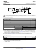
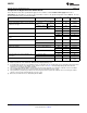
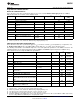
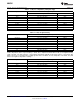
Pin PIN # D1 D2 D3 D4 D5 D6 D7 R1 SNP ESD
Name CLAMP
V
DD
1 x x
D1+ 2 x
(1)
x x x x x x
D1− 3 x x x x x x x x
D2+ 4 x x x x x x x
D2- 6 x x x x x x x x
SMBDAT 7 x x x x x
SMBCLK 8 x x x
(1) Note: An “x” indicates that the component exists for the designated pin. SNP refers to a snap-back device.
Figure 3. ESD Protection Input Structure
6 Submit Documentation Feedback Copyright © 2004–2013, Texas Instruments Incorporated
Product Folder Links: LM95221