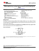
LMC7101, LMC7101Q www.ti.com SNOS719F – SEPTEMBER 1999 – REVISED MARCH 2013 LMC7101/LMC7101Q Tiny Low Power Operational Amplifier with Rail-to-Rail Input and Output Check for Samples: LMC7101, LMC7101Q FEATURES 1 • 2 • • • • • Tiny 5-Pin SOT-23 Package Saves Space—Typical Circuit Layouts Take Half the Space of 8-Pin SOIC Designs Guaranteed Specs at 2.7V, 3V, 5V, 15V Supplies Typical Supply Current 0.5 mA at 5V Typical Total Harmonic Distortion of 0.01% at 5V 1.
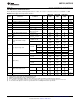
LMC7101, LMC7101Q SNOS719F – SEPTEMBER 1999 – REVISED MARCH 2013 www.ti.com Absolute Maximum Ratings (1) (2) ESD Tolerance (3) Human Body Model 1000V Machine Model 200V Charged Device Model 1000V Difference Input Voltage ±Supply Voltage (V+) + 0.3V, (V−) − 0.3V Voltage at Input/Output Pin Supply Voltage (V+ − V−) 16V Current at Input Pin Current at Output Pin ±5 mA (4) ±35 mA Current at Power Supply Pin 35 mA Lead Temp. (Soldering, 10 sec.
LMC7101, LMC7101Q www.ti.com SNOS719F – SEPTEMBER 1999 – REVISED MARCH 2013 2.7V Electrical Characteristics (continued) Unless otherwise specified, all limits guaranteed for TJ = 25°C, V+ = 2.7V, V− = 0V, VCM = VO = V+/2 and RL > 1 MΩ. Boldface limits apply at the temperature extremes. Symbol Parameter PSRR Power Supply Rejection Ratio CIN Common-Mode Input Capacitance Conditions V+ = 1.35V to 1.65V V− = −1.35V to −1.
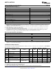
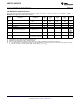
LMC7101, LMC7101Q SNOS719F – SEPTEMBER 1999 – REVISED MARCH 2013 www.ti.com 5V DC Electrical Characteristics Unless otherwise specified, all limits guaranteed for TJ = 25°C, V+ = 5V, V− = 0V, VCM = 1.5V, VO = V+/2 and RL = 1 MΩ. Boldface limits apply at the temperature extremes. Symbol Parameter Typ Conditions (1) LMC7101AI Limit LMC7101BI Limit LMC7101Q Limit 3 5 7 9 7 9 (2) 0.
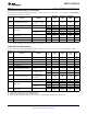
LMC7101, LMC7101Q www.ti.com SNOS719F – SEPTEMBER 1999 – REVISED MARCH 2013 15V DC Electrical Characteristics Unless otherwise specified, all limits guaranteed for TJ = 25°C, V+ = 15V, V− = 0V, VCM = 1.5V, VO = V+/2 and RL = 1 MΩ. Boldface limits apply at the temperature extremes. Symbol Parameter Conditions Typ (1) LMC7101AI Limit (2) LMC7101BI Limit (2) LMC7101Q Limit (2) (3) Units VOS Input Offset Voltage 0.11 mV max TCVOS Input Offset Voltage Average Drift 1.
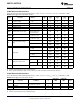
LMC7101, LMC7101Q SNOS719F – SEPTEMBER 1999 – REVISED MARCH 2013 www.ti.com 15V AC Electrical Characteristics Unless otherwise specified, all limits guaranteed for TJ = 25°C, V+ = 15V, V− = 0V, VCM = 1.5V, VO = V+/2 and RL = 1 MΩ. Boldface limits apply at the temperature extremes. Symbol Parameter Conditions Typ (1) LMC7101AI Limit LMC7101BI Limit LMC7101Q Limit Units 0.5 0.4 0.5 0.4 0.5 0.4 V/μs min (2) (2) (2) (3) Slew Rate (4) V+ = 15V 1.1 GBW Gain-Bandwidth Product V+ = 15V 1.
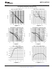
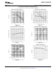
LMC7101, LMC7101Q www.ti.com SNOS719F – SEPTEMBER 1999 – REVISED MARCH 2013 2.7V Typical Performance Characteristics V = 2.7V, V− = 0V, TA = 25°C, unless otherwise specified. + Open Loop Frequency Response Input Voltage vs. Output Voltage Figure 2. Figure 3. Gain and Phase vs. Capacitance Load Gain and Phase vs. Capacitance Load Figure 4. Figure 5. dVOS vs. Supply Voltage dVOS vs. Common Mode Voltage Figure 6. Figure 7.
LMC7101, LMC7101Q SNOS719F – SEPTEMBER 1999 – REVISED MARCH 2013 www.ti.com 2.7V Typical Performance Characteristics (continued) + − V = 2.7V, V = 0V, TA = 25°C, unless otherwise specified. 8 Sinking Current vs. Output Voltage Sourcing Current vs. Output Voltage Figure 8. Figure 9.
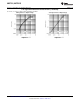
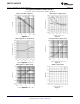
LMC7101, LMC7101Q www.ti.com SNOS719F – SEPTEMBER 1999 – REVISED MARCH 2013 3V Typical Performance Characteristics V = 3V, V− = 0V, TA = 25°C, unless otherwise specified. + Open Loop Frequency Response Input Voltage vs. Output Voltage Figure 10. Figure 11. Input Voltage Noise vs. Input Voltage Sourcing Current vs. Output Voltage Figure 12. Figure 13. Sinking Current vs. Output Voltage CMRR vs. Input Voltage Figure 14. Figure 15.
LMC7101, LMC7101Q SNOS719F – SEPTEMBER 1999 – REVISED MARCH 2013 www.ti.com 5V Typical Performance Characteristics V = 5V, V− = 0V, TA = 25°C, unless otherwise specified. + 10 Open Loop Frequency Response Input Voltage vs. Output Voltage Figure 16. Figure 17. Input Voltage Noise vs. Input Voltage Sourcing Current vs, Output Voltage Figure 18. Figure 19. Sinking Current vs. Output Voltage CMRR vs. Input Voltage Figure 20. Figure 21.
LMC7101, LMC7101Q www.ti.com SNOS719F – SEPTEMBER 1999 – REVISED MARCH 2013 15V Typical Performance Characteristics V = +15V, V− = 0V, TA = 25°C, unless otherwise specified. + Open Loop Frequency Response Input Voltage vs. Output Voltage Figure 22. Figure 23. Input Voltage Noise vs. Input Voltage Sourcing Current vs. Output Voltage Figure 24. Figure 25.
LMC7101, LMC7101Q SNOS719F – SEPTEMBER 1999 – REVISED MARCH 2013 www.ti.com 15V Typical Performance Characteristics (continued) + − V = +15V, V = 0V, TA = 25°C, unless otherwise specified. 12 Sinking Current vs. Output Voltage CMRR vs. Input Voltage Figure 26. Figure 27. Supply Current vs. Supply Voltage Input Current vs. Temperature Figure 28. Figure 29. Output Voltage Swing vs. Supply Voltage Input Voltage Noise vs. Frequency Figure 30. Figure 31.
LMC7101, LMC7101Q www.ti.com SNOS719F – SEPTEMBER 1999 – REVISED MARCH 2013 15V Typical Performance Characteristics (continued) + − V = +15V, V = 0V, TA = 25°C, unless otherwise specified. Positive PSRR vs. Frequency Negative PSRR vs. Frequency Figure 32. Figure 33. CMRR vs. Frequency Open Loop Frequency Response @ −40°C Figure 34. Figure 35. Open Loop Frequency Response @ 25°C Open Loop Frequency Response @ 85°C Figure 36. Figure 37.
LMC7101, LMC7101Q SNOS719F – SEPTEMBER 1999 – REVISED MARCH 2013 www.ti.com 15V Typical Performance Characteristics (continued) + − V = +15V, V = 0V, TA = 25°C, unless otherwise specified. 14 Maximum Output Swing vs. Frequency Gain and Phase vs. Capacitive Load Figure 38. Figure 39. Gain and Phase vs. Capacitive Load Output Impedance vs. Frequency Figure 40. Figure 41. Slew Rate vs. Temperature Slew Rate vs. Supply Voltage Figure 42. Figure 43.
LMC7101, LMC7101Q www.ti.com SNOS719F – SEPTEMBER 1999 – REVISED MARCH 2013 15V Typical Performance Characteristics (continued) + − V = +15V, V = 0V, TA = 25°C, unless otherwise specified. Inverting Small Signal Pulse Response Inverting Small Signal Pulse Response Figure 44. Figure 45. Inverting Small Signal Pulse Response Inverting Large Signal Pulse Response Figure 46. Figure 47. Inverting Large Signal Pulse Response Inverting Large Signal Pulse Response Figure 48. Figure 49.
LMC7101, LMC7101Q SNOS719F – SEPTEMBER 1999 – REVISED MARCH 2013 www.ti.com 15V Typical Performance Characteristics (continued) + − V = +15V, V = 0V, TA = 25°C, unless otherwise specified. 16 Non-Inverting Small Signal Pulse Response Non-Inverting Small Signal Pulse Response Figure 50. Figure 51. Non-Inverting Small Signal Pulse Response Non-Inverting Large Signal Pulse Response Figure 52. Figure 53.
LMC7101, LMC7101Q www.ti.com SNOS719F – SEPTEMBER 1999 – REVISED MARCH 2013 15V Typical Performance Characteristics (continued) + − V = +15V, V = 0V, TA = 25°C, unless otherwise specified. Stability vs. Capacitive Load Stability vs. Capacitive Load Figure 56. Figure 57. Stability vs. Capacitive Load Stability vs. Capacitive Load Figure 58. Figure 59. Stability vs. Capacitive Load Stability vs. Capacitive Load Figure 60. Figure 61.
LMC7101, LMC7101Q SNOS719F – SEPTEMBER 1999 – REVISED MARCH 2013 www.ti.com APPLICATION INFORMATION BENEFITS OF THE LMC7101 TINY AMP Size The small footprint of the SOT-23-5 packaged Tiny amp, (0.120 x 0.118 inches, 3.05 x 3.00 mm) saves space on printed circuit boards, and enable the design of smaller electronic products. Because they are easier to carry, many customers prefer smaller and lighter products. Height The height (0.056 inches, 1.
LMC7101, LMC7101Q www.ti.com SNOS719F – SEPTEMBER 1999 – REVISED MARCH 2013 An input voltage signal exceeds the LMC7101 power supply voltages with no output phase inversion. Figure 62. Input Voltage A ±7.5V input signal greatly exceeds the 3V supply in Figure 64 causing no phase inversion due to RI. Figure 63. Input Signal Applications that exceed this rating must externally limit the maximum input current to ±5 mA with an input resistor as shown in Figure 64. Figure 64.
LMC7101, LMC7101Q SNOS719F – SEPTEMBER 1999 – REVISED MARCH 2013 www.ti.com Figure 65. Resistive Isolation of a 330 pF Capacitive Load COMPENSATING FOR INPUT CAPACITANCE WHEN USING LARGE VALUE FEEDBACK RESISTORS When using very large value feedback resistors, (usually > 500 kΩ) the large feed back resistance can react with the input capacitance due to transducers, photo diodes, and circuit board parasitics to reduce phase margins.
LMC7101, LMC7101Q www.ti.com SNOS719F – SEPTEMBER 1999 – REVISED MARCH 2013 REVISION HISTORY Changes from Revision E (March 2013) to Revision F • Page Changed layout of National Data Sheet to TI format ..........................................................................................................
PACKAGE OPTION ADDENDUM www.ti.
PACKAGE OPTION ADDENDUM www.ti.com (4) 1-Nov-2013 There may be additional marking, which relates to the logo, the lot trace code information, or the environmental category on the device. (5) Multiple Device Markings will be inside parentheses. Only one Device Marking contained in parentheses and separated by a "~" will appear on a device. If a line is indented then it is a continuation of the previous line and the two combined represent the entire Device Marking for that device.
PACKAGE MATERIALS INFORMATION www.ti.com 26-Mar-2013 TAPE AND REEL INFORMATION *All dimensions are nominal Device Package Package Pins Type Drawing SPQ Reel Reel A0 Diameter Width (mm) (mm) W1 (mm) B0 (mm) K0 (mm) P1 (mm) LMC7101AIM5 SOT-23 DBV 5 1000 178.0 8.4 LMC7101AIM5/NOPB SOT-23 DBV 5 1000 178.0 LMC7101AIM5X SOT-23 DBV 5 3000 178.
PACKAGE MATERIALS INFORMATION www.ti.com 26-Mar-2013 *All dimensions are nominal Device Package Type Package Drawing Pins SPQ Length (mm) Width (mm) Height (mm) LMC7101AIM5 SOT-23 DBV 5 1000 210.0 185.0 35.0 LMC7101AIM5/NOPB SOT-23 DBV 5 1000 210.0 185.0 35.0 LMC7101AIM5X SOT-23 DBV 5 3000 210.0 185.0 35.0 LMC7101AIM5X/NOPB SOT-23 DBV 5 3000 210.0 185.0 35.0 LMC7101BIM5 SOT-23 DBV 5 1000 210.0 185.0 35.0 LMC7101BIM5/NOPB SOT-23 DBV 5 1000 210.0 185.
IMPORTANT NOTICE Texas Instruments Incorporated and its subsidiaries (TI) reserve the right to make corrections, enhancements, improvements and other changes to its semiconductor products and services per JESD46, latest issue, and to discontinue any product or service per JESD48, latest issue. Buyers should obtain the latest relevant information before placing orders and should verify that such information is current and complete.