LMF100 LMF100 High Performance Dual Switched Capacitor Filter Literature Number: SNOSBG9A
LMF100 High Performance Dual Switched Capacitor Filter General Description The LMF100 consists of two independent general purpose high performance switched capacitor filters. With an external clock and 2 to 4 resistors, various second-order and first-order filtering functions can be realized by each filter block. Each block has 3 outputs. One output can be configured to perform either an allpass, highpass, or notch function. The other two outputs perform bandpass and lowpass functions.
LMF100 Absolute Maximum Ratings (Note 1) J Package: 10 sec. 300˚C SO Package: Vapor Phase (60 sec.) 215˚C Infrared (15 sec.) 220˚C See AN-450 “Surface Mounting Methods and Their Effect on Product Reliability” (Appendix D) for other methods of soldering surface mount devices. If Military/Aerospace specified devices are required, please contact the National Semiconductor Sales Office/ Distributors for availability and specifications. (Note 14) Supply Voltage (V+ − V−) Voltage at Any Pin 16V V+ + 0.
(Continued) The following specifications apply for Mode 1, Q = 10 (R1 = R3 = 100k, R2 = 10k), V+ = +5V and V− = −5V unless otherwise specified. Boldface limits apply for TMIN to TMAX; all other limits TA = TJ = 25˚C.
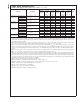
LMF100 Logic Input Characteristics Boldface limits apply for TMIN to TMAX; all other limits TA = TJ = 25˚C. LMF100CCN Parameter Conditions LMF100CIWM Typical Tested Design Typical Tested Design (Note 8) Limit Limit (Note 8) Limit Limit (Note 10) Units (Note 9) (Note 10) (Note 9) CMOS Clock MIN Logical “1” V+ = +5V, V− = −5V, +3.0 +3.0 +3.0 Input Voltage MAX Logical “0” VLSh = 0V −3.0 −3.0 −3.0 V MIN Logical “1” V+ = +10V, V− = 0V, +8.0 +8.0 +8.
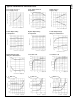
LMF100 Typical Performance Characteristics Power Supply Current vs Power Supply Voltage Power Supply Current vs Temperature DS005645-40 Positive Output Swing vs Temperature Output Swing vs Supply Voltage DS005645-41 Negative Output Swing vs Temperature DS005645-43 Negative Output Voltage Swing vs Load Resistance DS005645-42 Positive Output Voltage Swing vs Load Resistance DS005645-44 DS005645-45 fCLK/f0 Ratio vs Q fCLK/f0 Ratio vs Q DS005645-48 DS005645-47 DS005645-46 fCLK/f0 Ratio vs fCLK
LMF100 Typical Performance Characteristics fCLK/f0 Ratio vs fCLK (Continued) fCLK/f0 Ratio vs Temperature Q Deviation vs Clock Frequency DS005645-55 Q Deviation vs Clock Frequency Q Deviation vs Clock Frequency DS005645-56 Q Deviation vs Temperature DS005645-59 DS005645-58 www.national.
Maximum f0 vs Q at Vs = ± 7.5V LMF100 Typical Performance Characteristics (Continued) Maximum f0 vs Q at Vs = ± 5.0V DS005645-61 Maximum f0 vs Q at Vs = ± 2.5V DS005645-62 DS005645-63 LMF100 System Block Diagram DS005645-1 7 www.national.
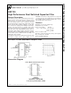
LMF100 Pin Descriptions LP(1,20), BP(2,19), N/AP/HP(3,18) INV(4,17) LSh(9) The second order lowpass, bandpass and notch/allpass/highpass outputs. These outputs can typically swing to within 1V of each supply when driving a 5 kΩ load. For optimum performance, capacitive loading on these outputs should be minimized. For signal frequencies above 15 kHz the capacitance loading should be kept below 30 pF.
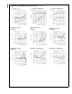
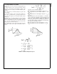
LMF100 1.0 Definitions of Terms fCLK: the frequency of the external clock signal applied to pin 10 or 11. f0: center frequency of the second order function complex pole pair. f0 is measured at the bandpass outputs of the LMF100, and is the frequency of maximum bandpass gain. (Figure 1). fnotch: the frequency of minimum (ideally zero) gain at the notch outputs. fz: the center frequency of the second order complex zero pair, if any.
LMF100 1.0 Definitions of Terms (Continued) DS005645-21 DS005645-22 (a) (b) FIGURE 2. 2nd-Order Low-Pass Response DS005645-23 DS005645-24 (a) (b) FIGURE 3. 2nd-Order High-Pass Response www.national.
LMF100 1.0 Definitions of Terms (Continued) DS005645-25 DS005645-26 (a) (b) FIGURE 4. 2nd-Order Notch Response DS005645-27 DS005645-28 (a) (b) FIGURE 5. 2nd-Order All-Pass Response 11 www.national.
LMF100 1.0 Definitions of Terms (a) Bandpass (Continued) (b) Low Pass (c) High-Pass DS005645-64 (d) Notch DS005645-65 (e) All-Pass DS005645-67 DS005645-68 FIGURE 6. Response of various 2nd-order filters as a function of Q. Gains and center frequencies are normalized to unity. www.national.
LMF100 2.0 Modes of Operation The LMF100 is a switched capacitor (sampled data) filter. To fully describe its transfer functions, a time domain analysis is appropriate. Since this is cumbersome, and since the LMF100 closely approximates continuous filters, the following discussion is based on the well-known frequency domain. Each LMF100 can produce two full 2nd order functions. See Table 1 for a summary of the characteristics of the various modes.
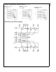
LMF100 2.0 Modes of Operation MODE 2: Notch 2, Bandpass, Lowpass: fnotch < f0 (Continued) (See Figure 10) MODE 1b: Notch 1, Bandpass, Lowpass Outputs: fnotch = f0 (See Figure 9) DS005645-14 FIGURE 9. MODE 1b DS005645-36 FIGURE 10. MODE 2 www.national.
MODE 3a: HP, BP, LP and Notch with External Op Amp (Continued) (See Figure 12) MODE 3: Highpass, Bandpass, Lowpass Outputs (See Figure 11) DS005645-5 *In Mode 3, the feedback loop is closed around the input summing amplifier; the finite GBW product of this op amp causes a slight Q enhancement. If this is a problem, connect a small capacitor (10 pF−100 pF) across R4 to provide some phase lead. FIGURE 11. MODE 3 15 www.national.com LMF100 2.
LMF100 2.0 Modes of Operation (Continued) DS005645-10 FIGURE 12. MODE 3a MODE 4: Allpass, Bandpass, Lowpass Outputs (See Figure 13) MODE 5: Numerator Complex Zeros, BP, LP (See Figure 14) *Due to the sampled data nature of the filter, a slight mismatch of fz and f0 occurs causing a 0.4 dB peaking around f0 of the allpass filter amplitude response (which theoretically should be a straight line). If this is unacceptable, Mode 5 is recommended. www.national.
LMF100 2.0 Modes of Operation (Continued) DS005645-6 FIGURE 13. MODE 4 DS005645-15 FIGURE 14. MODE 5 MODE 6a: Single Pole, HP, LP Filter (See Figure 15) DS005645-16 FIGURE 15. MODE 6a 17 www.national.
LMF100 2.0 Modes of Operation (Continued) DS005645-7 FIGURE 16. MODE 6b MODE 6c: Single Pole, AP, LP Filter (See Figure 17) MODE 6b: Single Pole LP Filter (Inverting and NonInverting) (See Figure 16) DS005645-17 FIGURE 17. MODE 6c www.national.
LMF100 2.0 Modes of Operation (Continued) DS005645-37 Equivalent Circuit DS005645-38 FIGURE 18. MODE 7 MODE 7: Summing Integrator (See Figure 18) 19 www.national.
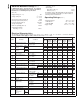
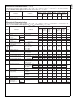
LMF100 2.0 Modes of Operation (Continued) TABLE 1. Summary of Modes. Realizable filter types (e.g. low-pass) denoted by asterisks. Unless otherwise noted, gains of various filter outputs are inverting and adjustable by resistor ratios. Mode BP LP 1 * * HP N AP * Number of Adjustable Resistors fCLK/f0 3 No 2 No 3 No (2) 1a May need input buffer. HOBP1 = −Q HOLP = + 1 Poor dynamics HOBP2 = + 1 1b Notes for high Q. * * * Useful for high frequency applications.
externally. From Table 1, we see that Mode 3 can be used to produce a low-pass filter with resistor-adjustable center frequency. (Continued) 3.1 DESIGN EXAMPLE In most filter designs involving multiple second-order stages, it is best to place the stages with lower Q values ahead of stages with higher Q, especially when the higher Q is greater than 0.707. This is due to the higher relative gain at the center frequency of a higher-Q stage.
LMF100 3.0 Applications Information (Continued) DS005645-30 FIGURE 19. Fourth-order Chebyshev low-pass filter from example in 3.1. ± 5V power supply. 0V–5V TTL or ± 5V CMOS logic levels. DS005645-31 FIGURE 20. Fourth-order Chebyshev low-pass filter from example in 3.1. Single +10V power supply. 0V–5V TTL logic levels. Input signals should be referred to half-supply or applied through a coupling capacitor. www.national.
LMF100 3.0 Applications Information (Continued) DS005645-33 DS005645-32 (a) Resistive Divider with Decoupling Capacitor (b) Voltage Regulator DS005645-34 (c) Operational Amplifier with Divider FIGURE 21. Three Ways of Generating V+/2 for Single-Supply Operation puts are not being directly used. Accompanying Figures 7, 8, 9, 10, 11, 12, 13, 14, 15, 16 and Figure 17 are equations labeled “circuit dynamics”, which relate the Q and the gains at the various outputs.
LMF100 3.0 Applications Information Mode 3 (Continued) Mode 1b Mode 2 and Mode 5 Mode 6a and 6c Mode 6b DS005645-12 FIGURE 22. Offset Voltage Sources In many applications, the outputs are ac coupled and dc offsets are not bothersome unless large signals are applied to the filter input. However, larger offset voltages will cause clipping to occur at lower ac signal levels, and clipping at any of the outputs will cause gain nonlinearities and will change f0 and Q.
LMF100 3.0 Applications Information (Continued) DS005645-39 R1 = 100 kΩ R2 = 1 kΩ R3 = 100 kΩ R4 = 100 kΩ Rg = 10 kΩ Rl = 10 kΩ Rh = 10 kΩ FIGURE 23. Second-Order Notch Filter DS005645-13 FIGURE 24. Method for Trimming VOS 3.5 SAMPLED DATA SYSTEM CONSIDERATIONS The LMF100 is a sampled data filter, and as such, differs in many ways from conventional continuous-time filters.
LMF100 3.0 Applications Information Performance Characteristics”. As Q is changed, the true value of the ratio changes as well. Unless the Q is low, the error in fCLK/f0 will be small. If the error is too large for a specific application, use a mode that allows adjustment of the ratio with external resistors. (Continued) signals. In noise-sensitive applications, a ratio of 100:1 will result in 3 dB lower output noise for the same filter configuration.
LMF100 Physical Dimensions inches (millimeters) unless otherwise noted Small Outline Package Order Number LMF100CIWM NS Package Number M20B Molded Dual-In-Line Package (N) Order Number LMF100CCN NS Package Number N20A 27 www.national.
LMF100 High Performance Dual Switched Capacitor Filter Notes LIFE SUPPORT POLICY NATIONAL’S PRODUCTS ARE NOT AUTHORIZED FOR USE AS CRITICAL COMPONENTS IN LIFE SUPPORT DEVICES OR SYSTEMS WITHOUT THE EXPRESS WRITTEN APPROVAL OF THE PRESIDENT AND GENERAL COUNSEL OF NATIONAL SEMICONDUCTOR CORPORATION. As used herein: 1.
IMPORTANT NOTICE Texas Instruments Incorporated and its subsidiaries (TI) reserve the right to make corrections, modifications, enhancements, improvements, and other changes to its products and services at any time and to discontinue any product or service without notice. Customers should obtain the latest relevant information before placing orders and should verify that such information is current and complete.