
Datasheet
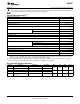
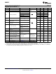
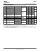
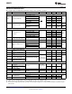

LMH0031
www.ti.com
SNLS218A –JANUARY 2006–REVISED APRIL 2013
LMH0031 SMPTE 292M/259M Digital Video Deserializer / Descrambler with Video
and Ancillary Data FIFOs
Check for Samples: LMH0031
1
FEATURES
APPLICATIONS
2
• SDTV/HDTV Serial Digital Video Standard
• SDTV/HDTV Serial-to-Parallel Digital Video
Compliant Interfaces for:
• Supports 270 Mbps, 360 Mbps, 540 Mbps, – Video Editing Equipment
1.483 Gbps and 1.485 Gbps Serial Video Data
– VTRs
Rates with Auto-Detection
– Standards Converters
• LSB De-Dithering Option
– Digital Video Routers and Switchers
• Uses Low-Cost 27MHz Crystal or Clock
– Digital Video Processing and Editing
Oscillator Reference
Equipment
• Fast VCO Lock Time: < 500 µs at 1.485 Gbps
– Video Test Pattern Generators and Digital
• Built-in Self-Test (BIST) and Video Test Pattern
Video Test Equipment
Generator (TPG)
– Video Signal Generators
(1)
Patent Applications Made or Pending
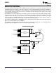
DESCRIPTION
• Automatic EDH/CRC Word and Flag
Processing
The LMH0031 SMPTE 292M / 259M Digital Video
Deserializer/Descrambler with Video and Ancillary
• Ancillary Data FIFO with Extensive Packet
Data FIFOs is a monolithic integrated circuit that
Handling Options
deserializes and decodes SMPTE 292M, 1.485Gbps
• Adjustable, 4-Deep Parallel Output Video Data
(or 1.483Gbps) serial component video data, to 20-bit
FIFO
parallel data with a synchronized parallel word-rate
clock. It also deserializes and decodes SMPTE 259M,
• Flexible Control and Configuration I/O Port
270Mbps, 360Mbps and SMPTE 344M (proposed)
• LVCMOS Compatible Control Inputs and Clock
540Mbps serial component video data, to 10-bit
and Data Outputs
parallel data. Functions performed by the LMH0031
• LVDS and ECL-Compatible, Differential, Serial
include: clock/data recovery from the serial data,
Inputs
serial-to-parallel data conversion, SMPTE standard
data decoding, NRZI-to-NRZ conversion, parallel data
• 3.3V I/O Power Supply and 2.5V Logic Power
clock generation, word framing, CRC and EDH data
Supply Operation
checking and handling, Ancillary Data extraction and
• Low Power: Typically 850mW
automatic video format determination. The parallel
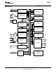
• 64-Pin TQFP Package
video output features a variable-depth FIFO which
can be adjusted to delay the output data up to 4
• Commercial Temperature Range 0°C to +70°C
parallel data clock periods. Ancillary Data may be
selectively extracted from the parallel data through
the use of masking and control bits in the
configuration and control registers and stored in the
on-chip FIFO. Reverse LSB dithering is also
implemented.
1
Please be aware that an important notice concerning availability, standard warranty, and use in critical applications of
Texas Instruments semiconductor products and disclaimers thereto appears at the end of this data sheet.
2All trademarks are the property of their respective owners.
PRODUCTION DATA information is current as of publication date.
Copyright © 2006–2013, Texas Instruments Incorporated
Products conform to specifications per the terms of the Texas
Instruments standard warranty. Production processing does not
necessarily include testing of all parameters.