
Datasheet

LMH0346
www.ti.com
SNLS248J –APRIL 2007–REVISED APRIL 2013
3 Gbps HD/SD SDI Reclocker with Dual Differential Outputs
Check for Samples: LMH0346
1
FEATURES
DESCRIPTION
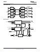
The LMH0346 3 Gbps HD/SD SDI Reclocker retimes
2
• Supports SMPTE 424M, SMPTE 292M, and
serial digital video data conforming to the SMPTE
SMPTE 259M (C) Serial Digital Video
424M, SMPTE 292M, and SMPTE 259M (C)
Standards
standards. The LMH0346 operates at serial data
• Supports 270 Mbps, 1.483 Gbps, 1.485 Gbps,
rates of 270 Mbps, 1.483 Gbps, 1.485 Gbps, 2.967
2.967 Gbps, and 2.97 Gbps Serial Data Rate
Gbps, and 2.97 Gbps. The LMH0346 supports DVB-
Operation
ASI operation at 270 Mbps.
• Supports DVB-ASI at 270 Mbps
The LMH0346 automatically detects the incoming
• Single 3.3V Supply Operation data rate and adjusts itself to retime the incoming
data to suppress accumulated jitter. The LMH0346
• 370 mW Typical Power Consumption
recovers the serial data-rate clock and optionally
• Two Differential, Reclocked Outputs
provides it as an output. The LMH0346 has two
• Choice of Second Reclocked Output or Low-
differential serial data outputs; the second output may
be selected as a low-jitter, data-rate clock output.
Jitter, Differential, Data-Rate Clock Output
Controls and indicators are: serial clock or second
• Single 27 MHz External Crystal or Reference
serial data output select, manual rate select input,
Clock Input
SD/HD rate indicator output, lock detect output,
• Manual or Automatic Rate Select Input
auto/manual data bypass and output mute. The serial
data inputs, outputs, and serial clock outputs are
• SD/HD Operating Rate Indicator Output
differential LVPECL compatible. The CML serial data
• Lock Detect Indicator Output
and serial clock outputs are suitable for driving 100Ω
• Output Mute Function for Data and Clock
differentially terminated networks. The control logic
• Auto/Manual Reclocker Bypass
inputs and outputs are LVCMOS compatible.
• Differential LVPECL Compatible Serial Data
The LMH0346 is powered from a single 3.3V supply.
Inputs and Outputs
Power dissipation is typically 370 mW.
• LVCMOS Control Inputs and Indicator Outputs
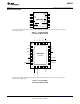
The device is available in two space-saving
• 20-Pin HTSSOP or 24-Pin WQFN Package
packages: a 6.5 X 4.4 mm 20-pin HTSSOP and an
even more space–efficient 5 X 4 mm 24-pin WQFN
• Industrial Temperature Range: -40°C to +85°C
package.
• Footprint Compatible With the LMH0046 and
LMH0026 (HTSSOP Package)
APPLICATIONS
• SDTV/HDTV and 3 Gbps Serial Digital Video
Interfaces for:
– Digital Video Routers and Switchers
– Digital Video Processing and Editing
Equipment
– DVB-ASI Equipment
– Video Standards and Format Converters
1
Please be aware that an important notice concerning availability, standard warranty, and use in critical applications of
Texas Instruments semiconductor products and disclaimers thereto appears at the end of this data sheet.
2All trademarks are the property of their respective owners.
PRODUCTION DATA information is current as of publication date.
Copyright © 2007–2013, Texas Instruments Incorporated
Products conform to specifications per the terms of the Texas
Instruments standard warranty. Production processing does not
necessarily include testing of all parameters.