
Datasheet
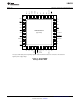

LMH0356
www.ti.com
SNLS270K –AUGUST 2007–REVISED APRIL 2013
3 Gbps HD/SD SDI Reclocker with 4:1 Input Mux and FR4 EQs
Check for Samples: LMH0356
1
FEATURES
DESCRIPTION
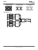
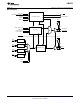
The LMH0356 3 Gbps HD/SD SDI Reclocker with 4:1
2
• Supports SMPTE 424M, SMPTE 292M, and
Input Mux and FR4 EQs retimes serial digital video
SMPTE 259M (C) Serial Digital Video
data conforming to the SMPTE 424M, SMPTE 292M,
Standards
and SMPTE 259M (C) standards. The LMH0356
• Supports 270 Mbps, 1.483 Gbps, 1.485 Gbps,
operates at serial data rates of 270 Mbps, 1.483
2.967 Gbps, and 2.97 Gbps Serial Data Rate
Gbps, 1.485 Gbps, 2.967 Gbps, and 2.97 Gbps. The
Operation
LMH0356 supports DVB-ASI operation at 270 Mbps.
The LMH0356 includes an integrated 4:1 input
• Supports DVB-ASI at 270 Mbps
multiplexer for selecting one of four input data
• Single 3.3V Supply Operation
streams for retiming. In addition, the four inputs of the
• 430 mW Typical Power Consumption
LMH0356 each have an FR4 equalizer capable of
equalizing 0-30” of FR4 trace length.
• Integrated 4:1 Multiplexed Input
• 0-30” FR4 Equalizer on Each Multiplexed Input
The LMH0356 automatically detects the incoming
data rate and adjusts itself to retime the incoming
• Two Differential, Reclocked Outputs
data to suppress accumulated jitter. The LMH0356
• Choice of Second Reclocked Output or
recovers the serial data-rate clock and optionally
Recovered Clock Output
provides it as an output. The LMH0356 has two
• Single 27 MHz External Crystal or Reference
differential serial data outputs; the second output may
be selected as a low-jitter, data-rate clock output.
Clock Input
Controls and indicators are: serial clock or second
• Manual Rate Select Input
serial data output select, manual rate select input,
• SD/HD Operating Rate Indicator Output
SD/HD rate indicator output, lock detect output,
• Lock Detect Indicator Output
auto/manual data bypass, output mute, and device
enable. The serial data inputs, outputs, and serial
• Output Mute Function for Data and Clock
clock outputs are differential LVPECL compatible.
• Auto/Manual Reclocker Bypass
The CML serial data and serial clock outputs are
• Power Saver Mode With Device Power Down
suitable for driving 100Ω differentially terminated
Control (10 mW Typical Power Consumption in
networks. The control logic inputs and outputs are
LVCMOS compatible.
Disabled State)
• Differential LVPECL Compatible Serial Data
The LMH0356 is powered from a single 3.3V supply.
Inputs and Outputs
Power dissipation is typically 430 mW. The device is
available in two space-saving packages: a 7 x 7 mm
• LVCMOS Control Inputs and Indicator Outputs
48-pin WQFN and even more space-efficient
• 48-Pin WQFN or 40-Pin WQFN Package
5 x 5 mm 40-pin WQFN package.
• Industrial Temperature Range: -40°C to +85°C
• 48-Pin WQFN Version Footprint Compatible
With the LMH0056 and LMH0036
APPLICATIONS
• SDTV/HDTV and 3 Gbps Serial Digital Video
Interfaces for:
– Digital Video Routers and Switchers
– Digital Video Processing and Editing
Equipment
– DVB-ASI Equipment
– Video Standards and Format Converters
1
Please be aware that an important notice concerning availability, standard warranty, and use in critical applications of
Texas Instruments semiconductor products and disclaimers thereto appears at the end of this data sheet.
2All trademarks are the property of their respective owners.
PRODUCTION DATA information is current as of publication date.
Copyright © 2007–2013, Texas Instruments Incorporated
Products conform to specifications per the terms of the Texas
Instruments standard warranty. Production processing does not
necessarily include testing of all parameters.