
Datasheet

LMH1982
www.ti.com
SNLS289C –APRIL 2008–REVISED MARCH 2013
LMH1982 Multi-Rate Video Clock Generator with Genlock
Check for Samples: LMH1982
1
FEATURES
DESCRIPTION
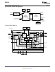
The LMH1982 is a multi-rate video clock generator
2
• Two Simultaneous LVDS Output Clocks with
ideal for use in a wide range of 3-Gbps (3G), high-
Selectable Frequencies and Hi-Z Capability:
definition (HD), and standard-definition (SD) video
– SD Clock: 27 MHz or 67.5 MHz
applications, such as video synchronization, serial
– HD Clock: 74.25 MHz, 74.25/1.001 MHz,
digital interface (SDI) serializer and deserializer
(SerDes), video conversion, video editing, and other
148.5 MHz or 148.5/1.001 MHz
broadcast and professional video systems.
• Low-Jitter Output Clocks May Be Directly
Connected to an FPGA Serializer to Meet
The LMH1982 can generate two simultaneous SD
SMPTE SDI Jitter Specifications and HD clocks and a Top of Frame (TOF) pulse. In
genlock mode, the device's phase locked loops
• Top of Frame (TOF) Pulse with Programmable
(PLLs) can synchronize the output signals to H sync
Output Format Timing and Hi-Z Capability
and V sync input signals applied to either of the
• Two reference ports (A and B) with H and V
reference ports. The input reference can have analog
sync inputs
timing from Texas Instrument's LMH1981 multi-format
video sync separator or digital timing from an SDI
• Supports Cross-Locking of Input and Output
deserializer and should conform to the major SD and
Timing
HD standards. When a loss of reference occurs, the
• External Loop Filter Allows Control of Loop
device can default to free run operation where the
Bandwidth, Jitter Transfer, and Lock Time
output timing accuracy will be determined by the
Characteristics
external bias on the free run control voltage input.
• Free Run or Holdover Operation on Loss of
The LMH1982 can replace discrete PLLs and field-
Reference
programmable gate array (FPGA) PLLs with multiple
• User-Defined Free Run Control Voltage Input
voltage controlled crystal oscillators (VCXOs). Only
one 27.0000 MHz VCXO and loop filter are externally
• I
2
C Interface and Control Registers
required for genlock mode. The external loop filter as
• 3.3V and 2.5V Supplies
well as programmable PLL parameters can provide
narrow loop bandwidths to minimize jitter transfer. HD
APPLICATIONS
clock output jitter as low as 40 ps peak-to-peak can
help designers using FPGA SerDes meet stringent
• Video Genlock and Synchronization
SDI output jitter specifications.
• FPGA SDI SerDes Recovered Clock
Generation
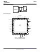
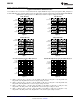
The LMH1982 is offered in a space-saving 5 mm x 5
mm 32-pin WQFN package and provides low total
• Triple Rate 3G/HD/SD-SDI SerDes
power consumption of about 250 mW (typical).
• Video Capture, Conversion, Editing and
Distribution
• Video Displays and Projectors
• Broadcast and Professional Video Equipment
1
Please be aware that an important notice concerning availability, standard warranty, and use in critical applications of
Texas Instruments semiconductor products and disclaimers thereto appears at the end of this data sheet.
2All trademarks are the property of their respective owners.
PRODUCTION DATA information is current as of publication date.
Copyright © 2008–2013, Texas Instruments Incorporated
Products conform to specifications per the terms of the Texas
Instruments standard warranty. Production processing does not
necessarily include testing of all parameters.