
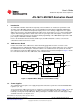
Datasheet

www.ti.com
Introduction
Table 3. Input Select Switch, SW2
ON OFF
• U7 buffer output is in Hi-Z mode • U7 buffer output is enabled
• LMH1981 sync signals is gated off from port REF_A • LMH1981 sync signals are passed to port REF_A
• External input signals can be applied to HIN_A and VIN_A
of header J8
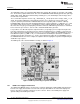
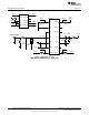
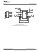
1.3.2 Digital Reference Input
In addition to the analog timing signals from the sync separator, external H and V sync input signals can
be applied to ports REF_A or REF_B via header J8. See Table 4 for the pin assignment of J8. Note:
Before applying external signals to HIN_A and VIN_A, set SW2 = ON to avoid signal conflict with the
LMH1981.
The external reference can have digital timing, such as from an SDI receiver or deserializer, and should
be a recognized timing format listed in Table 3 of the LMH1982 Multi-Rate Video Clock Generator with
Genlock Data Sheet (SNLS289). A 48 kHz audio clock can also be applied to the H sync input to
synchronize the output clocks.
Note: The H input frequency accuracy should be within the absolute pull range (APR) of the 27 MHz
VCXO (e.g. ±50 ppm) in order to phase lock the outputs to the input reference; otherwise, phase lock may
not be achieved.
Table 4. Input Header, J8
Pin # Pin Name Pin # Pin Name
1 GND 8 HIN_A
2 GND 7 VIN_A
3 GND 6 HIN_B
4 GND 5 VIN_B
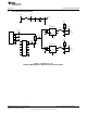
1.4 Output Clock
The LVDS output SD and HD clocks from the LMH1982 are routed via controlled 100Ω differential
impedance lines to edge-mount SMA connectors as indicated in Table 5. If a differential probe will be used
to measure the clocks directly on the board, then the differential lines should be terminated by populating
R37 and R38 with 100Ω. If the SMA connectors will be used to transmit the clock signal, these resistors
should not be populated; and termination should be done at the receiver instead.
To provide compatibility between various differential signaling levels and receivers, the board allows for
AC coupling capacitors C31/C34 and C35/C37 on the SD_CLK and HD_CLK differential pairs. AC
coupling allows for common-mode level translation/shifting at the receiver.
Table 5. LVDS Output Clock Ports, J3 – J6
LVDS SMA Port Clock Port Name
J3 / J4 SD_CLK / SD_CLK
J5 / J6 HD_CLK / HD_CLK
1.5 Output Top of Frame
The output top of frame (TOF) pulse from the LMH1982 can be measured at test point TP23 and at
header J10 located at the bottom edge of the board. The TOF output is a 3.3V LVCMOS signal. The total
load capacitance on the TOF output should be less than 15 pF.
3
SNOA527A–May 2008–Revised April 2013 AN-1841 LMH1982 Evaluation Board
Submit Documentation Feedback
Copyright © 2008–2013, Texas Instruments Incorporated