
Datasheet
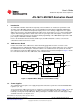

Introduction
www.ti.com
1.6 27 MHZ VCXO and Loop Filter
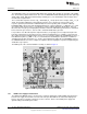
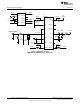
The LMH1982 requires an external 27 MHz VCXO (X1) and loop filter circuitry for operation of the VCXO
PLL. The board is populated with a CTS 357-series 27.0000 MHz VCXO with ±50 ppm absolute pull range
(APR), which yields 1000 Hz/V nominal tuning sensitivity (K
VCO
). The VCXO input control voltage can be
measured at test point TP21.
The second-order loop filter consists of R
S
= 20 kΩ (R8), C
S
= 44 μF (C10 = C27 = 22 μF), and C
P
= 1 μF
(C28). The parallel combination of C10 and C27 form the series capacitor, C
S
. Based on the loop
response equations provided in the LMH1982 datasheet, this loop filter yields a nominal -3 dB loop
bandwidth (BW) of about 3 Hz and nominal damping factor of 0.8 assuming K
VCO
= 1000 Hz/V, I
CP1
= 250
μA (charge pump current for PLL 1), and FB_DIV = 1716 (feedback divider for NTSC input). This loop
filter was chosen to give good output jitter performance when the LMH1982 is genlocked to a clean black
burst or tri-level sync reference, such as from a Tektronix TG700 video generator.
It is possible to use different loop filter component values (or topologies) to meet output clock jitter and
lock time requirements for other input reference signals and applications. For example, to generate low-
jitter output clock from a high-jitter input reference (e.g. recovered H signal from an FPGA SDI receiver), a
narrowband loop filter (e.g. BW < 1 Hz ) is recommended for maximum jitter attenuation. In addition to
changing the loop filter components, I
CP1
can also be programmed to adjust the loop bandwidth. Refer to
the LMH1982 datasheet for more complete descriptions about designing the loop filter and optimizing the
VCXO PLL loop response.
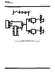
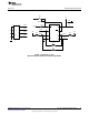
The PCB layout of the external VCXO PLL circuitry is shown in Figure 2.
Figure 2. PCB Layout showing Loop Filter and VCXO
1.6.1 VCXO Power Supply Considerations
The VCXO and LMP7701 devices operate from a separate supply plane (VDD_VCXO) derived from the
board’s 3.3V supply. Resistor R5 is used to form a low-pass filter with the associated decoupling and
bypass capacitors to attenuate supply noise to these devices. Refer to the VCXO power supply and
ground routing in the PCB layout section.
4
AN-1841 LMH1982 Evaluation Board SNOA527A–May 2008–Revised April 2013
Submit Documentation Feedback
Copyright © 2008–2013, Texas Instruments Incorporated