
Datasheet
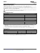


-0.5
0 0.5 1 1.5
V
G
(V)
GAIN (dB)
2
-90
-80
-70
-60
-50
-40
30
-30
-20
-10
0
10
20
0
1
2
3
4
5
12
6
7
8
9
10
11
GAIN
(
V
/
V
)
dB
(V/V)
-55°C
25°C
125°C
-55°C
25°C
125°C
V
IN
1
8
3
2
5
4
7
6
R
F
1 k:
R
L
100:
R
G
100:
V
-
V
+
V
G
LMH6504
www.ti.com
SNOSA96D –NOVEMBER 2003–REVISED MARCH 2013
LMH6504 Wideband, Low Power, Variable Gain Amplifier
Check for Samples: LMH6504
1
FEATURES
DESCRIPTION
The LMH™6504 is a wideband DC coupled voltage
23
• V
S
= ±5V, T
A
= 25°C, R
F
= 1 KΩ, R
G
= 100Ω, R
L
controlled gain stage followed by a high-speed
= 100Ω, A
V
= A
VMAX
= 9.7V/V, Typical values
current feedback Op Amp which can directly drive a
unless specified.
low impedance load. Gain adjustment range is 80 dB
• −3 dB BW 150 MHz
for up to 10 MHz by varying the gain control input
voltage, V
G
.
• Gain control BW 150 MHz
• Adjustment range (<10 MHz) 80 dB
Maximum gain is set by external components, and
the gain can be reduced all the way to cut-off. Power
• Output offset voltage ±55 mV
consumption is 110 mW with a speed of 150 MHz
• Gain matching (limit) ±0.42 dB
and a gain control bandwidth (BW) of 150 MHz.
• Supply voltage range 7V to 12V
Output referred DC offset voltage is less than 55 mV
over the entire gain control voltage range. Device-to-
• Slew rate (inverting) 1500 V/μs
device gain matching is within ±0.42 dB at maximum
• Supply Current (no load) 11 mA
gain. Furthermore, gain is tested over a wide range.
• Linear Output Current ±60 mA
The output current feedback Op Amp allows high
• Output Voltage Swing ±2.2V
frequency large signals (Slew Rate > 1500 V/μs) and
can also drive a heavy load current (60 mA). Near
• Input Noise Voltage 4.4 nV/√Hz
ideal input characteristics (i.e. low input bias current,
• Input Noise Current 2.6 pA/√Hz
low offset, low pin 3 resistance) enable the device to
• THD (20 MHz, R
L
= 100Ω, V
O
= 2 V
PP
) −45 dBc
be easily configured as an inverting amplifier as well
(see Application Information section for details).
• Replacement for CLC5523
To provide ease of use when working with a single
APPLICATIONS
supply, V
G
range is set to be from 0V to +2V relative
to the ground pin potential (pin 4). V
G
input
• Variable attenuator
impedance is high in order to ease drive requirement.
• AGC
In single supply operation, the ground pin is tied to a
• Voltage controlled filter
"virtual" half supply.
• Video imaging processing
Typical Application
Figure 1. Gain vs. V
G
Figure 2. A
VMAX
= 9.7 V/V
1
Please be aware that an important notice concerning availability, standard warranty, and use in critical applications of
Texas Instruments semiconductor products and disclaimers thereto appears at the end of this data sheet.
2LMH is a trademark of Texas Instruments.
3All other trademarks are the property of their respective owners.
PRODUCTION DATA information is current as of publication date.
Copyright © 2003–2013, Texas Instruments Incorporated
Products conform to specifications per the terms of the Texas
Instruments standard warranty. Production processing does not
necessarily include testing of all parameters.