
Datasheet
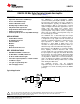
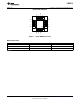
Table Of Contents
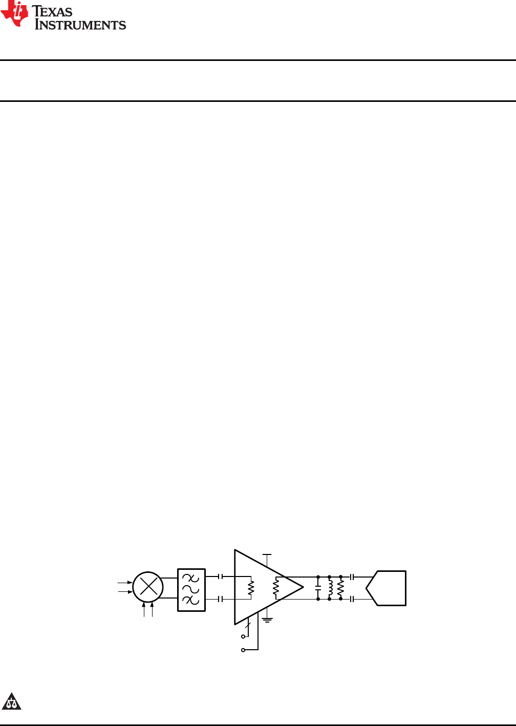
GAIN
200
ADC14155
R
OUT
3
LATCH
RF
LO
LMH6514
V
CC
R
LOAD
LMH6514
www.ti.com
SNOSB06A –JANUARY 2008–REVISED MARCH 2013
LMH6514 600 MHz, Digital Controlled, Variable Gain Amplifier
Check for Samples: LMH6514
1
FEATURES
DESCRIPTION
The LMH6514 is a high performance, digitally
2
• Adjustable Gain with a 42 dB Range
controlled variable gain amplifier (DVGA). It combines
• Precise 6.02 dB Gain Steps
precision gain control with a low noise, ultra-linear,
• Parallel 3 Bit Gain Control
differential amplifier. Typically, the LMH6514 drives a
high performance ADC in a broad range of mixed
• On Chip Register Gain Setting
signal and digital communication applications such as
• Fully Differential Signal Path
mobile radio and cellular base stations where
• Single Ended to Differential Capable
automatic gain control (AGC) is required to increase
system dynamic range. When used in conjunction
• 200Ω Input Impedance
with a high speed ADC, system dynamic range can
• Small Footprint (4 mm x 4 mm) WQFN Package
be extended by up to 42 dB.
The LMH6514 has a differential input and output
APPLICATIONS
allowing large signal swings on a single 5V supply. It
• Cellular Base Stations
is designed to accept signals from RF elements and
• IF Sampling Receivers
maintain a terminated impedance environment. The
input impedance is 200Ω resistive. The output
• Instrumentation
impedance is either 200Ω or 400Ω and is user
• Modems
selectable. A unique internal architecture allows use
• Imaging
with both single ended and differential input signals.
• Differential Line Receiver
Input signals to the LMH6514 are scaled by a highly
linear, digitally controlled attenuator with seven
KEY SPECIFICATIONS
accurate 6 dB steps. The attenuator output provides
the input signal for a high gain, ultra linear differential
• 600 MHz bandwidth at 100Ω load
transconductor. The transconductor differential output
• 39 dBm OIP3 at 75 MHz, 200Ω load
current can be converted into a voltage by using the
• 26 dB to 38 dB maximum gain
on-chip 200Ω or 400Ω loads. The transconductance
gain is 0.1 Amp/Volt resulting in a maximum voltage
• Selectable output impedance of 200Ω or 400Ω.
gain of +32 dB when driving a 200Ω load, or 38 dB
• 8.3 dB noise figure
when driving the 400Ω load.
• 5 ns gain step switching time
The LMH6514 operates over the industrial
• 100 mA supply current
temperature range of −40°C to +85°C. The LMH6514
is available in a 16-Pin, thermally enhanced, WQFN
package.
Typical Application
1
Please be aware that an important notice concerning availability, standard warranty, and use in critical applications of
Texas Instruments semiconductor products and disclaimers thereto appears at the end of this data sheet.
2All trademarks are the property of their respective owners.
PRODUCTION DATA information is current as of publication date.
Copyright © 2008–2013, Texas Instruments Incorporated
Products conform to specifications per the terms of the Texas
Instruments standard warranty. Production processing does not
necessarily include testing of all parameters.