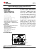
LMH6518 www.ti.com SNOSB21C – MAY 2008 – REVISED JULY 2013 LMH6518 900 MHz, Digitally Controlled, Variable Gain Amplifier Check for Samples: LMH6518 FEATURES DESCRIPTION • • • The LMH6518 is a digitally controlled variable gain amplifier whose total gain can be varied from −1.16 dB to 38.8 dB for a 40 dB range in 2 dB steps. The −3 dB bandwidth is 900 MHz at all gains. Gain accuracy at each setting is typically 0.1 dB.
LMH6518 SNOSB21C – MAY 2008 – REVISED JULY 2013 www.ti.com These devices have limited built-in ESD protection. The leads should be shorted together or the device placed in conductive foam during storage or handling to prevent electrostatic damage to the MOS gates. Absolute Maximum Ratings ESD Tolerance (1) (2) (3) Human Body Model 2000V Machine Model 200V Charge Device Model 1000V Supply Voltage VCC (5V nominal) 5.5V VDD (3.3V nominal) 3.
LMH6518 www.ti.com SNOSB21C – MAY 2008 – REVISED JULY 2013 Electrical Characteristics (1) (continued) Unless otherwise specified, all limits are ensured for TA = 25°C, Input CM = 2.5V, VCM = 1.2V, VCM_Aux = 1.2V, Single-ended input drive, VCC = 5V, VDD = 3.3V, RL = 100Ω differential (both Main & Auxiliary Outputs), VOUT = 0.7 VPP differential (both Main & Auxiliary Outputs), both Main and Auxiliary Output Specifications, full bandwidth setting, gain = 18.
LMH6518 SNOSB21C – MAY 2008 – REVISED JULY 2013 www.ti.com Electrical Characteristics (1) (continued) Unless otherwise specified, all limits are ensured for TA = 25°C, Input CM = 2.5V, VCM = 1.2V, VCM_Aux = 1.2V, Single-ended input drive, VCC = 5V, VDD = 3.3V, RL = 100Ω differential (both Main & Auxiliary Outputs), VOUT = 0.7 VPP differential (both Main & Auxiliary Outputs), both Main and Auxiliary Output Specifications, full bandwidth setting, gain = 18.
LMH6518 www.ti.com SNOSB21C – MAY 2008 – REVISED JULY 2013 Table 1. Definition of Terms and Specifications 1. AV_CM (dB) Change in output offset voltage (ΔVOOS) with respect to the change in input common mode voltage (ΔVI_CM) 2. AV_DIFF (dB) Gain with 100Ω differential load 3. CM Common Mode 4. CMRR (dB) Common Mode rejection defined as: AV_DIFF (dB) - AV_CM (dB) 5. CMRR_CM Common ΔVOOS /ΔVCM 6. HG Preamp High Gain 7. Ladder Ladder Attenuator setting (0-20 dB) 8.
LMH6518 SNOSB21C – MAY 2008 – REVISED JULY 2013 www.ti.
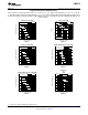
LMH6518 www.ti.com SNOSB21C – MAY 2008 – REVISED JULY 2013 Typical Performance Characteristics Unless otherwise specified, Input CM = 2.5V, VCM = 1.2V, VCM AUX = 1.2V, Single-ended input drive, VCC = 5V, VDD = 3.3V, RL = 100Ω differential (both Main & Auxiliary Outputs), VOUT = 0.7 VPP differential (both Main and Auxiliary Outputs), Main output specification (Auxiliary is labeled “Auxiliary”), full bandwidth setting, gain = 18.8 dB (Preamp LG, 0 dB ladder attenuation), Full Power setting (1).
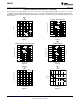
LMH6518 SNOSB21C – MAY 2008 – REVISED JULY 2013 www.ti.com Typical Performance Characteristics (continued) Unless otherwise specified, Input CM = 2.5V, VCM = 1.2V, VCM AUX = 1.2V, Single-ended input drive, VCC = 5V, VDD = 3.3V, RL = 100Ω differential (both Main & Auxiliary Outputs), VOUT = 0.7 VPP differential (both Main and Auxiliary Outputs), Main output specification (Auxiliary is labeled “Auxiliary”), full bandwidth setting, gain = 18.8 dB (Preamp LG, 0 dB ladder attenuation), Full Power setting (1).
LMH6518 www.ti.com SNOSB21C – MAY 2008 – REVISED JULY 2013 Typical Performance Characteristics (continued) Unless otherwise specified, Input CM = 2.5V, VCM = 1.2V, VCM AUX = 1.2V, Single-ended input drive, VCC = 5V, VDD = 3.3V, RL = 100Ω differential (both Main & Auxiliary Outputs), VOUT = 0.7 VPP differential (both Main and Auxiliary Outputs), Main output specification (Auxiliary is labeled “Auxiliary”), full bandwidth setting, gain = 18.8 dB (Preamp LG, 0 dB ladder attenuation), Full Power setting (1).
LMH6518 SNOSB21C – MAY 2008 – REVISED JULY 2013 www.ti.com Typical Performance Characteristics (continued) Unless otherwise specified, Input CM = 2.5V, VCM = 1.2V, VCM AUX = 1.2V, Single-ended input drive, VCC = 5V, VDD = 3.3V, RL = 100Ω differential (both Main & Auxiliary Outputs), VOUT = 0.7 VPP differential (both Main and Auxiliary Outputs), Main output specification (Auxiliary is labeled “Auxiliary”), full bandwidth setting, gain = 18.8 dB (Preamp LG, 0 dB ladder attenuation), Full Power setting (1).
LMH6518 www.ti.com SNOSB21C – MAY 2008 – REVISED JULY 2013 APPLICATIONS INFORMATION FUNCTIONAL DESCRIPTION AND DYNAMIC RANGE IN OSCILLOSCOPE APPLICATIONS Here is a block diagram of the LMH6518’s Main Output signal path: 50: +In Ladder Attenuator 10 Steps, 2 dB/ Step Pre-amp 10 dB or 30 dB 0 to -20 dB -In +Out Output Amp 8.86 dB -Out 50: Figure 57. LMH6518 Signal Path Block Diagram The Auxiliary output (not shown) uses another but similar Output Amp that taps into the Ladder Attenuator output.
LMH6518 SNOSB21C – MAY 2008 – REVISED JULY 2013 www.ti.com Assuming a nominal 0.7VPP output, the LMH6518’s minimum FS input swing is limited by the maximum signal path gain possible and vice versa: 0.7 VPP Minimum LMH6518 FS Input = (38.8 + 1.41) dB = 6.8 mVPP 10 20 (4) (or 8 mVPP with no ADC fine adjust) Maximum LMH6518 FS Input = 10 0.7 VPP (-1.16 ± 1.
LMH6518 www.ti.com SNOSB21C – MAY 2008 – REVISED JULY 2013 22 20 58 18 56 16 54 14 52 12 50 10 48 8 46 6 44 4 42 2 40 38 0.001 Preamp LG 0 -2 Preamp HG 0.01 0.1 LADDER ATTENUATION (dB) SNR (dBFS) 62 60 200 MHz Filter 1 INPUT FS (V) Figure 58. LMH6518 SNR & Ladder Attenuation used vs. Input As can be seen from Figure 58, SNR of at least 52 dB is maintained for FS inputs above 24 mVPP (3 mV/DIV on a scope) assuming the LMH6518’s internal 200 MHz filter is enabled.
LMH6518 SNOSB21C – MAY 2008 – REVISED JULY 2013 www.ti.com One possible attenuation partitioning is to select the additional attenuator value to cover a 20 dB range above 0.8 VPP FS (to 8 VPP) with the 100x attenuator covering the remaining 20 dB range from 8 VPP to 80 VPP. Mapping 8 VPP FS scope input to 0.8 VPP at LMH6518 input means the additional attenuator is 10x, as shown in Table 2, Row 4.
LMH6518 www.ti.com SNOSB21C – MAY 2008 – REVISED JULY 2013 The “1.05” factor is to add 5% FS overhead margin to avoid ADC overdrive. 16.8 Sx8 x 1.05 x 1020 = 639.3 mV FSE = 10 (13) Required condition: 0.56V ≤ FSE ≤ 0.84V Recommend condition: 0.595V ≤ FSE ≤ 0.805V for optimum ADC FS 5. Determine the ADC ECM code ratio: FSE - 0.56 ECM (ratio) = 0.28 where • • • 0.28V= (0.84-0.56)V 0.56V is the lower end of the ADC FS adjustability For this example: ECM (ratio) = 0.6393 - 0.56 = 0.283 0.
LMH6518 SNOSB21C – MAY 2008 – REVISED JULY 2013 www.ti.com C1 1 nF J1 Input (from 50: source) (2.5V CM) +IN R1 +5V R2 R5 100: LMH6518 49.9: 200: -IN R4 C2 200: R3 1 nF 24.9: Figure 59. Recommended Single-Ended Bench-Test Input Drive from 50Ω Source With the schematic of Figure 59, each LMH6518 input sees 25Ω to ground at the higher frequencies when the capacitors look like shorts.
LMH6518 www.ti.com SNOSB21C – MAY 2008 – REVISED JULY 2013 0.43 VPP, 1.2V DC +5V -5V 0.35 VPP, 0V DC R1 R3 0.7 VPP, 1.2V DC 50: +OUT Vx R2 VOUT To ADC R2 41.4: 50: -OUT LMH6518 R3 R1 131.3: 172.7: +5V -5V Figure 61. Output CM Shift Scheme With the scheme of Figure 61, Vx is kept at 1.2V, by proper selection of external resistor values, so that the LMH6518 outputs are not CM-loaded. As was the case with input level shifting, this output level shifting also consumes additional power (0.58W).
LMH6518 SNOSB21C – MAY 2008 – REVISED JULY 2013 www.ti.
LMH6518 www.ti.com SNOSB21C – MAY 2008 – REVISED JULY 2013 2400 RL = 100: AUXILIARY VOLTAGE (mV) 2200 VCM_Aux = 1.2V No CM Load 2000 +OUT Aux and -OUT Aux 85°C 1800 25°C 1600 1400 -40°C 1200 1000 4.5 4.7 4.9 5.1 5.3 5.5 VCC (V) Figure 63.
LMH6518 SNOSB21C – MAY 2008 – REVISED JULY 2013 SCLK 1 2 www.ti.com 3 8 4 24 9 25 CS Command Field LMH6518 Bus in Tri-State SDIO XXX Data Field C7 C6 C5 C4 C3 C2 C1 C0 1 X X X X X X X MSB Inter-Access Gap LSB 16 bits D15 D1 D0 LMH6518 Bus in Tri-State XXX Single Access Cycle Figure 64.
LMH6518 www.ti.com SNOSB21C – MAY 2008 – REVISED JULY 2013 Table 4. Data Field Filter D15 (MSB) D14 D13 D12 D11 X 0 0 0 0 D10 D9 0=Full Power 1=Aux Hi-Z 0 D8 D7 Pre-amp D6 See Table 6 D5 D4 0 0=LG 1=HG Ladder Attenuation D3 D2 D1 D0 (LSB) See Table 7 NOTE Bits D5, D9, D11-D14 must be “0”. Otherwise, device operation is undefined and specifications are not ensured. Table 5.
LMH6518 SNOSB21C – MAY 2008 – REVISED JULY 2013 www.ti.com Table 7. Ladder Attenuation Data Field (continued) Ladder Attenuation 1 1 Ladder Attenuation (dB) 1 1 Unallowed NOTE An “Unallowed” SPI-1 state may result in undefined operation where device behavior is not ensured.
LMH6518 www.ti.com SNOSB21C – MAY 2008 – REVISED JULY 2013 +5V +5V 3,4 U1 LMH6518 1 2 R11 R12 237: 237: +5V +OUT Aux 6 -OUT Aux 1 16 5,8 +5V VCM_Aux R1 R2 75: 75: + 5 4 U2 LMH7220 - 2 R10 100: 3 Trigger Output (LVDS) R3 3.83 k: 1% +5V R4 1.20 k: 1% U4 LP3985 2.5V 0-2.5V VA VREF VOUT SDA SCL U3 DAC101 C085 10 bit DAC 2 (I C) Figure 68.
LMH6518 SNOSB21C – MAY 2008 – REVISED JULY 2013 www.ti.
LMH6518 www.ti.com SNOSB21C – MAY 2008 – REVISED JULY 2013 For a flat frequency response, the DC (low frequency) gain needs to be lowered to match the less-than-1 V/V AC (high frequency) path gain through the JFETs. This can be done by increasing the value of R2. By choosing the values of R15 and R11 so that R21 R15 = R14 R11 (19) the frequency response at J10 Gate (and consequently the output) will remain flat when C7 starts to conduct.
LMH6518 SNOSB21C – MAY 2008 – REVISED JULY 2013 www.ti.com 12 SNR IMPACT (dB) 10 8 6 LNA Noise = 3 nV/ Hz 4 2 LNA Noise = 1.5 nV/ Hz 0 -2 2 6 10 14 18 22 26 30 34 38 42 GAIN (dB) Figure 70. LNA Buffer SNR Impact ATTENUATOR DESIGN Figure 71 shows a front-end attenuator designed to work with the JFET LNA of Figure 69. 1:1 10:1 C5 2-5 pF 100:1 C6 2-5 pF R1 900 k: C1 8 pF R2 111 k: C2 65 pF R3 990 k: C3 8 pF R4 10.
LMH6518 www.ti.com SNOSB21C – MAY 2008 – REVISED JULY 2013 REVISION HISTORY Hooman: Corrected PSRR condition from "HG" to "LG" per CMS C1305178. Changes from Revision A (March 2013) to Revision B • Page Changed layout of National Data Sheet to TI format ..........................................................................................................
PACKAGE OPTION ADDENDUM www.ti.
PACKAGE OPTION ADDENDUM www.ti.com 24-Jul-2013 In no event shall TI's liability arising out of such information exceed the total purchase price of the TI part(s) at issue in this document sold by TI to Customer on an annual basis.
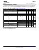
PACKAGE MATERIALS INFORMATION www.ti.com 24-Jul-2013 TAPE AND REEL INFORMATION *All dimensions are nominal Device Package Package Pins Type Drawing LMH6518SQ/NOPB WQFN RGH 16 LMH6518SQE/NOPB WQFN RGH LMH6518SQX/NOPB WQFN RGH SPQ Reel Reel A0 Diameter Width (mm) (mm) W1 (mm) B0 (mm) K0 (mm) P1 (mm) W Pin1 (mm) Quadrant 1000 178.0 12.4 4.3 4.3 1.3 8.0 12.0 Q1 16 250 178.0 12.4 4.3 4.3 1.3 8.0 12.0 Q1 16 4500 330.0 12.4 4.3 4.3 1.3 8.0 12.
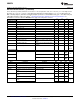
PACKAGE MATERIALS INFORMATION www.ti.com 24-Jul-2013 *All dimensions are nominal Device Package Type Package Drawing Pins SPQ Length (mm) Width (mm) Height (mm) LMH6518SQ/NOPB WQFN RGH 16 1000 213.0 191.0 55.0 LMH6518SQE/NOPB WQFN RGH 16 250 213.0 191.0 55.0 LMH6518SQX/NOPB WQFN RGH 16 4500 367.0 367.0 35.
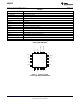
MECHANICAL DATA RGH0016A SQA16A (Rev A) www.ti.
IMPORTANT NOTICE Texas Instruments Incorporated and its subsidiaries (TI) reserve the right to make corrections, enhancements, improvements and other changes to its semiconductor products and services per JESD46, latest issue, and to discontinue any product or service per JESD48, latest issue. Buyers should obtain the latest relevant information before placing orders and should verify that such information is current and complete.