LMH6601, LMH6601-Q1 www.ti.com SNOSAK9E – JUNE 2006 – REVISED MARCH 2013 LMH6601/LMH6601Q 250 MHz, 2.4V CMOS Operational Amplifier with Shutdown Check for Samples: LMH6601, LMH6601-Q1 FEATURES DESCRIPTION • The LMH6601 is a low voltage (2.4V – 5.5V), high speed voltage feedback operational amplifier suitable for use in a variety of consumer and industrial applications.
LMH6601, LMH6601-Q1 SNOSAK9E – JUNE 2006 – REVISED MARCH 2013 www.ti.com These devices have limited built-in ESD protection. The leads should be shorted together or the device placed in conductive foam during storage or handling to prevent electrostatic damage to the MOS gates. ABSOLUTE MAXIMUM RATINGS ESD Tolerance (2) (1) Human Body Model 2 kV Machine Model 200V VIN Differential Input Current ±2.5V (3) ±10 mA Output Current 200 mA Supply Voltage (V+ – V−) (4) 6.
LMH6601, LMH6601-Q1 www.ti.com SNOSAK9E – JUNE 2006 – REVISED MARCH 2013 5V ELECTRICAL CHARACTERISTICS Single Supply with VS= 5V, AV = +2, RF = 604Ω, SD tied to V+, VOUT = VS/2, RL = 150Ω to V− unless otherwise specified. Boldface limits apply at temperature extremes. (1) Symbol Parameter Condition Min (2) Typ (2) Max (2) Units Frequency Domain Response SSBW –3 dB Bandwidth Small Signal SSBW_1 VOUT = 0.25 VPP 130 VOUT = 0.25 VPP, AV = +1 250 MHz Peak Peaking VOUT = 0.
LMH6601, LMH6601-Q1 SNOSAK9E – JUNE 2006 – REVISED MARCH 2013 www.ti.com 5V ELECTRICAL CHARACTERISTICS (continued) Single Supply with VS= 5V, AV = +2, RF = 604Ω, SD tied to V+, VOUT = VS/2, RL = 150Ω to V− unless otherwise specified. Boldface limits apply at temperature extremes. (1) Symbol Parameter Condition Min (2) 0V ≤ VIN ≤ 3.5V Typ (2) Max (2) 10 Units RIN Input Resistance CIN Input Capacitance 1.
LMH6601, LMH6601-Q1 www.ti.com SNOSAK9E – JUNE 2006 – REVISED MARCH 2013 3.3V ELECTRICAL CHARACTERISTICS Single Supply with VS= 3.3V, AV = +2, RF = 604Ω, SD tied to V+, VOUT = VS/2, RL = 150Ω to V− unless otherwise specified. Boldface limits apply at temperature extremes. (1) Symbol Parameter Condition Min (2) Typ (2) Max (2) Units Frequency Domain Response SSBW –3 dB Bandwidth Small Signal SSBW_1 VOUT = 0.25 VPP 125 VOUT = 0.25 VPP, AV = +1 250 Peak Peaking VOUT = 0.
LMH6601, LMH6601-Q1 SNOSAK9E – JUNE 2006 – REVISED MARCH 2013 www.ti.com 3.3V ELECTRICAL CHARACTERISTICS (continued) Single Supply with VS= 3.3V, AV = +2, RF = 604Ω, SD tied to V+, VOUT = VS/2, RL = 150Ω to V− unless otherwise specified. Boldface limits apply at temperature extremes. (1) Symbol IB Parameter Condition Input Bias Current See Min (2) (4) (4) Typ (2) Max 5 50 2 25 (2) Units pA IOS Input Offset Current See RIN Input Resistance 0V ≤ VIN ≤ 1.8V CIN Input Capacitance 1.
LMH6601, LMH6601-Q1 www.ti.com SNOSAK9E – JUNE 2006 – REVISED MARCH 2013 2.7V ELECTRICAL CHARACTERISTICS Single Supply with VS = 2.7V, AV = +2, RF = 604Ω, SD tied to V+, VOUT = VS/2, RL = 150Ω to V− unless otherwise specified. Boldface limits apply at temperature extremes. (1) Symbol Parameter Condition Min (2) Typ (2) Max (2) Units Frequency Domain Response SSBW –3 dB Bandwidth Small Signal SSBW_1 VOUT = 0.25 VPP 120 VOUT = 0.25 VPP, AV = +1 250 MHz Peak Peaking VOUT = 0.
LMH6601, LMH6601-Q1 SNOSAK9E – JUNE 2006 – REVISED MARCH 2013 www.ti.com 2.7V ELECTRICAL CHARACTERISTICS (continued) Single Supply with VS = 2.7V, AV = +2, RF = 604Ω, SD tied to V+, VOUT = VS/2, RL = 150Ω to V− unless otherwise specified. Boldface limits apply at temperature extremes.
LMH6601, LMH6601-Q1 www.ti.com SNOSAK9E – JUNE 2006 – REVISED MARCH 2013 CONNECTION DIAGRAM 6 1 OUTPUT 5 V - 2 + +IN 3 V + SD - 4 -IN Figure 2.
LMH6601, LMH6601-Q1 SNOSAK9E – JUNE 2006 – REVISED MARCH 2013 www.ti.com TYPICAL PERFORMANCE CHARACTERISTICS Unless otherwise noted, all data is with AV = +2, RF = RG = 604Ω, VS = 3.3V, VOUT = VS/2, SD tied to V+, RL = 150Ω to V−, T = 25°C. 3 3 80 VS = 5V GAIN 40 0 0.25 VPP -40 -6 1 VPP -9 -80 2 VPP -12 -120 -15 -18 1 10 PHASE (°) 0 -3 PHASE 100 VS = 3.3V GAIN NORMALIZED GAIN (dB) 0 NORMALIZED GAIN (dB) Frequency Response for Various Output Amplitudes 80 40 0.
LMH6601, LMH6601-Q1 www.ti.com SNOSAK9E – JUNE 2006 – REVISED MARCH 2013 TYPICAL PERFORMANCE CHARACTERISTICS (continued) Unless otherwise noted, all data is with AV = +2, RF = RG = 604Ω, VS = 3.3V, VOUT = VS/2, SD tied to V+, RL = 150Ω to V−, T = 25°C. Frequency Response for Various Supply Voltages 6 6 30 VOUT = 0.25 VPP 3 NORMALIZED GAIN (dB) NORMALIZED GAIN (dB) 3 RL TIED TO V0 1 k: -3 50: -6 150: -9 -12 0 3.3V 0 -3 10 100 -60 -6 -90 -9 -120 2.7V -12 -150 3.
LMH6601, LMH6601-Q1 SNOSAK9E – JUNE 2006 – REVISED MARCH 2013 www.ti.com TYPICAL PERFORMANCE CHARACTERISTICS (continued) Unless otherwise noted, all data is with AV = +2, RF = RG = 604Ω, VS = 3.3V, VOUT = VS/2, SD tied to V+, RL = 150Ω to V−, T = 25°C. Peak Output Swing vs. RL Output Swing vs. Sink Current for Various Supply Voltages 2.5 1 5V 3.3V - 3.3V VOUT FROM V (V) PEAK SWING (VP) 2 1.5 2.7V 1 AV = +5 V/V 5V 0.1 RL to VS/2 VOUT_DC = VS/2 0.
LMH6601, LMH6601-Q1 www.ti.com SNOSAK9E – JUNE 2006 – REVISED MARCH 2013 TYPICAL PERFORMANCE CHARACTERISTICS (continued) Unless otherwise noted, all data is with AV = +2, RF = RG = 604Ω, VS = 3.3V, VOUT = VS/2, SD tied to V+, RL = 150Ω to V−, T = 25°C. THD vs. Output Swing -20 Slew Rate vs. Ambient Temperature 310 RL = 1 k: to VS/2 -30 SLEW RATE (V/Ps) -40 -50 THD (dBc) 5V, FALLING 290 VS = 3.3V -60 10 MHz -70 -80 270 3.3V, FALLING 250 5V, RISING 230 3.
LMH6601, LMH6601-Q1 SNOSAK9E – JUNE 2006 – REVISED MARCH 2013 www.ti.com TYPICAL PERFORMANCE CHARACTERISTICS (continued) Unless otherwise noted, all data is with AV = +2, RF = RG = 604Ω, VS = 3.3V, VOUT = VS/2, SD tied to V+, RL = 150Ω to V−, T = 25°C. Closed Loop Output Impedance vs. Frequency for Various Supply Voltages Off Isolation vs. Frequency 0 100 VS = 5V AV = +1 -10 ISOLATION (dB) -20 |ZOUT| (:) 10 2.7V 3.
LMH6601, LMH6601-Q1 www.ti.com SNOSAK9E – JUNE 2006 – REVISED MARCH 2013 TYPICAL PERFORMANCE CHARACTERISTICS (continued) Unless otherwise noted, all data is with AV = +2, RF = RG = 604Ω, VS = 3.3V, VOUT = VS/2, SD tied to V+, RL = 150Ω to V−, T = 25°C. −PSRR vs. Frequency 80 Supply Current vs. Ambient Temperature 10 3.3V 2.7V 70 9.8 9.4 5V 50 IS (mA) -PSRR (dB) 5V 9.6 60 40 30 3.3V 9.2 9 2.7V 8.8 20 8.6 10 8.4 8.
LMH6601, LMH6601-Q1 SNOSAK9E – JUNE 2006 – REVISED MARCH 2013 www.ti.com TYPICAL PERFORMANCE CHARACTERISTICS (continued) Unless otherwise noted, all data is with AV = +2, RF = RG = 604Ω, VS = 3.3V, VOUT = VS/2, SD tied to V+, RL = 150Ω to V−, T = 25°C. Offset Voltage vs. VCM (Typical Part) Input Bias Current vs. Common Mode Voltage 4 1000 125°C 85°C 2 25°C 100 125° OPERATION IS NOT RECOMMENDED -2 10 |IB| (pA) VIO (mV) 0 -40°C -4 1 25°C -6 .1 VS = 3.3V -8 - VCM MEASURED FROM V 0 0.
LMH6601, LMH6601-Q1 www.ti.com SNOSAK9E – JUNE 2006 – REVISED MARCH 2013 TYPICAL PERFORMANCE CHARACTERISTICS (continued) Unless otherwise noted, all data is with AV = +2, RF = RG = 604Ω, VS = 3.3V, VOUT = VS/2, SD tied to V+, RL = 150Ω to V−, T = 25°C. DG vs. VOUT for Various VS 0.2 DP vs. VOUT for Various VS 0.2 - VS = 5V RL = 150: TO V DC COUPLED DG MEASURED RELATIVE 0.1 0 -0.1 DP (°) DG (%) 0.1 TO V OUT = VS/2 IN EACH CASE 0 VS = 5V VS = 2.5V - -0.3 -0.
LMH6601, LMH6601-Q1 SNOSAK9E – JUNE 2006 – REVISED MARCH 2013 www.ti.com APPLICATION INFORMATION OPTIMIZING PERFORMANCE With many op amps, additional device non-linearity and sometimes less loop stability arises when the output has to switch from current-source mode to current-sink mode or vice versa.
LMH6601, LMH6601-Q1 www.ti.com SNOSAK9E – JUNE 2006 – REVISED MARCH 2013 V + + V IL-MAX LMH6601 VO LMH6601 RP V VO CO RP RL RL - V (a) DUAL SUPPLY (b) AC COUPLED LOAD § V-1 RP d RL ¨ ¨VO_MIN © § ¨ ¨ © VO_MIN is the most negative swing at output RP d VO_MIN IL_MAX VO_MIN is the most negative swing at output and IL_MAX is maximum load current with direction shown Figure 49.
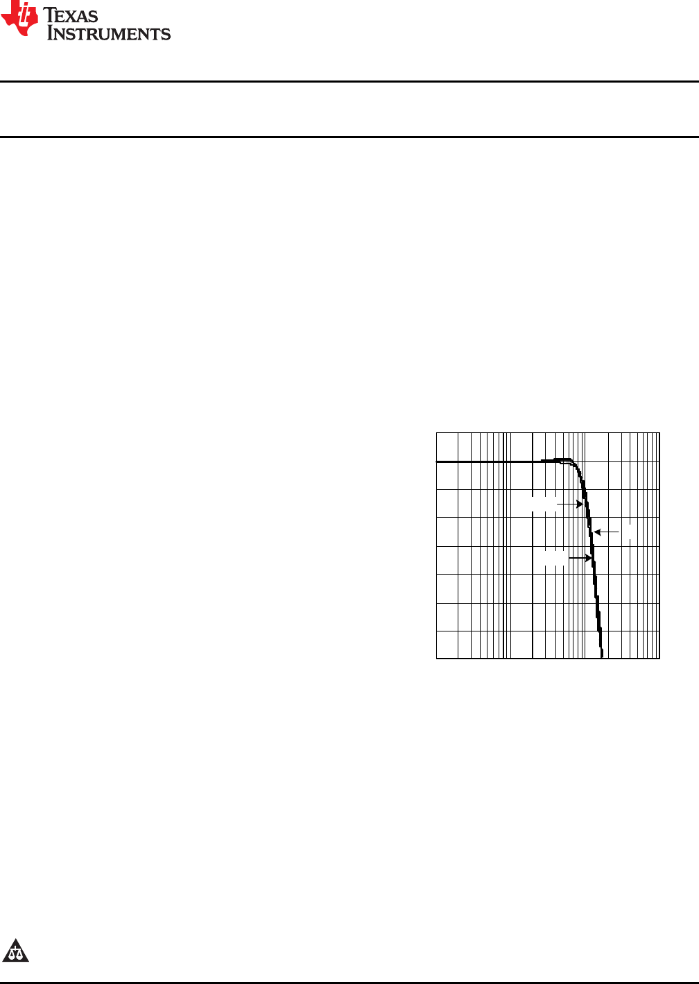
LMH6601, LMH6601-Q1 SNOSAK9E – JUNE 2006 – REVISED MARCH 2013 www.ti.com OVERLOAD RECOVERY AND SWING CLOSE TO RAILS The LMH6601 can recover from an output overload in less than 20 ns. See Figure 50 below for the input and output scope photos: (VOLTS) VS = ±2.5V INPUT (4 VPP) OUTPUT (1V/DIV) TIME (10 ns/DIV) Figure 50.
LMH6601, LMH6601-Q1 www.ti.com SNOSAK9E – JUNE 2006 – REVISED MARCH 2013 SINGLE SUPPLY VIDEO APPLICATION The LMH6601’s high speed and fast slew rate make it an ideal choice for video amplifier and buffering applications. There are cost benefits in having a single operating supply. Single supply video systems can take advantage of the LMH6601’s low supply voltage operation along with its ability to operate with input common mode voltages at or slightly below the V− rail.
LMH6601, LMH6601-Q1 SNOSAK9E – JUNE 2006 – REVISED MARCH 2013 www.ti.com VIDEO DAC CURRENT OUTPUT COMPOSITE VIDEO IN 0-1V VS = 3.3V + iO 75: VLOAD LMH6601 U1 - RS 75: RL 75: RF 620: RG 620: Figure 53. Single Supply Composite Video Driver for Consumer Video Outputs If the “Video In” signal is Composite Video with negative going Sync tip, a variation of the previous configurations should be used.
LMH6601, LMH6601-Q1 www.ti.com SNOSAK9E – JUNE 2006 – REVISED MARCH 2013 Table 1. Finding Figure 54 External Resistor Values by Iteration Estimate RG (Ω) Calculated (from Equation 2) R3 (Ω) Equation 1 LHS Calculated Comment (Compare Equation 1 LHS Calculated to RHS) 1k 1.69k 0.988 Increase Equation 1 LHS by reducing RG 820 1.56k 1.15 Increase Equation 1 LHS by reducing RG 620 1.37k 1.45 Increase Equation 1 LHS by reducing RG 390 239 4.18 Reduce Equation 1 LHS by increasing RG 560 1.
LMH6601, LMH6601-Q1 SNOSAK9E – JUNE 2006 – REVISED MARCH 2013 www.ti.com VCC_5V CIN 0.47 PF R1 510 k: VCC_5V + VIN RT 75: R2 510 k: LMH6601 U1 CO 68 PF VO RO 75: + - CABLE VL - R4 2 k: C1 22 PF R3 1 k: RL 75: + - R5 680: Figure 56. AC Coupled Video Amplifier/Driver with SAG Compensation In this circuit, the output coupling capacitor value and size is reduced at the expense of a slightly more complicated circuitry.
LMH6601, LMH6601-Q1 www.ti.com SNOSAK9E – JUNE 2006 – REVISED MARCH 2013 4.0V (+) CLIPPING (A) 50% DUTY CYCLE NO CLIPPING 2Vp-p 2.5V 1.0V (-) CLIPPING 4.0V (+) CLIPPING (B) LOW DUTY CYCLE CLIPPED POSITIVE 2Vp-p 2.5V 1.0V (-) CLIPPING 4.0V (+) CLIPPING (C) HIGH DUTY CYCLE CLIPPED NEGATIVE 2.5V 2Vp-p 1.0V (-) CLIPPING Figure 58.
LMH6601, LMH6601-Q1 SNOSAK9E – JUNE 2006 – REVISED MARCH 2013 www.ti.com For any video line rate (HxV corresponding to the number of Active horizontal and vertical lines), the speed requirements can be estimated if the Horizontal Active (KH%) and Vertical Active (KV%) numbers are known. These percentages correspond to the percentages of the active number of lines (horizontal or vertical) to the total number of lines as set by VESA standards.
LMH6601, LMH6601-Q1 www.ti.com SNOSAK9E – JUNE 2006 – REVISED MARCH 2013 With the LMH6601 input bias current in the femto-amperes range, even large values of gain (RF) do not increase the output error term appreciably. This allows circuit operation to a lower light intensity level which is always of special importance in these applications.
LMH6601, LMH6601-Q1 SNOSAK9E – JUNE 2006 – REVISED MARCH 2013 www.ti.com Figure 61 shows that placing a capacitor, CF, with the proper value, across RF will create a pole in the NG function at fP. For optimum performance, this capacitor is usually picked so that NG is equal to the op amp's open loop gain at fP.
LMH6601, LMH6601-Q1 www.ti.com SNOSAK9E – JUNE 2006 – REVISED MARCH 2013 OTHER APPLICATIONS RF = 10 M: to 10 G: RS = 1 M: or SMALLER FOR HIGH COUNTING RATES CF = 1 pF CD = 1 pF to 10 PF VOUT = Q/CF WHERE Q is CHARGE CREATED BY ONE PHOTON or PARTICLE ADJUST VBIAS FOR MAXIMUM SNR CF RF 10 k: CD RS LMH6601 U1 + - VBIAS D1 1000 pF VOUT + Figure 62.
LMH6601, LMH6601-Q1 SNOSAK9E – JUNE 2006 – REVISED MARCH 2013 www.ti.com Table 4.
LMH6601, LMH6601-Q1 www.ti.com SNOSAK9E – JUNE 2006 – REVISED MARCH 2013 REVISION HISTORY Changes from Revision D (March 2013) to Revision E • Page Changed layout of National Data Sheet to TI format ..........................................................................................................
PACKAGE OPTION ADDENDUM www.ti.
PACKAGE OPTION ADDENDUM www.ti.
PACKAGE MATERIALS INFORMATION www.ti.com 21-Mar-2013 TAPE AND REEL INFORMATION *All dimensions are nominal Device Package Package Pins Type Drawing SPQ Reel Reel A0 Diameter Width (mm) (mm) W1 (mm) B0 (mm) K0 (mm) P1 (mm) W Pin1 (mm) Quadrant LMH6601MG/NOPB SC70 DCK 6 1000 178.0 8.4 2.25 2.45 1.2 4.0 8.0 Q3 LMH6601MGX/NOPB SC70 DCK 6 3000 178.0 8.4 2.25 2.45 1.2 4.0 8.0 Q3 LMH6601QMG/NOPB SC70 DCK 6 1000 178.0 8.4 2.25 2.45 1.2 4.0 8.
PACKAGE MATERIALS INFORMATION www.ti.com 21-Mar-2013 *All dimensions are nominal Device Package Type Package Drawing Pins SPQ Length (mm) Width (mm) Height (mm) LMH6601MG/NOPB SC70 DCK 6 1000 210.0 185.0 35.0 LMH6601MGX/NOPB SC70 DCK 6 3000 210.0 185.0 35.0 LMH6601QMG/NOPB SC70 DCK 6 1000 210.0 185.0 35.0 LMH6601QMGX/NOPB SC70 DCK 6 3000 210.0 185.0 35.
IMPORTANT NOTICE Texas Instruments Incorporated and its subsidiaries (TI) reserve the right to make corrections, enhancements, improvements and other changes to its semiconductor products and services per JESD46, latest issue, and to discontinue any product or service per JESD48, latest issue. Buyers should obtain the latest relevant information before placing orders and should verify that such information is current and complete.