
Datasheet
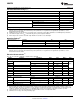


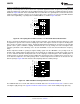

1M
10M 100M 1G
FREQUENCY (Hz)
-7
-6
-5
-4
-3
-2
-1
0
1
GAIN (dB)
-430
-380
-330
-280
-230
-180
-130
-80
-30
PHASE
(
°
)
A
V
= -1
A
V
= -10
A
V
= -4
A
V
= -2
V
OUT
= 2V
PP
R
F
= 237:
R
L
= 100:
PHASE
GAIN
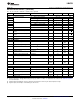
1M
10M 100M
FREQUENCY (Hz)
-105
-100
-95
-90
-85
-80
-75
-70
-65
-60
-40
HD (dBc)
-55
-50
-45
2V
PP
A
V
= +2
R
F
= 237:
HD2, R
L
= 100:
HD3, R
L
= 100:
HD2, R
L
= 1k:
HD3, R
L
= 1k:
LMH6702
www.ti.com
SNOSA03F –NOVEMBER 2002–REVISED MARCH 2013
LMH6702 1.7 GHz, Ultra Low Distortion, Wideband Op Amp
Check for Samples: LMH6702
1
FEATURES
DESCRIPTION
The LMH6702 is a very wideband, DC coupled
23
V
S
= ±5V, T
A
= 25°C, A
V
= +2V/V, R
L
= 100Ω,
monolithic operational amplifier designed specifically
V
OUT
= 2V
PP
, Typical Unless Noted:
for wide dynamic range systems requiring exceptional
• 2
nd
/3
rd
Harmonics (5MHz, SOT-23) −100/−96dBc
signal fidelity. Benefiting from current feedback
• −3dB Bandwidth (V
OUT
= 0.5 V
PP
) 1.7 GHz
architecture, the LMH6702 offers unity gain stability at
exceptional speed without need for external
• Low Noise 1.83nV/√Hz
compensation.
• Fast Settling to 0.1% 13.4ns
With its 720MHz bandwidth (A
V
= 2V/V, V
O
= 2V
PP
),
• Fast Slew Rate 3100V/μs
10-bit distortion levels through 60MHz (R
L
= 100Ω),
• Supply Current 12.5mA
1.83nV/√Hz input referred noise and 12.5mA supply
• Output Current 80mA
current, the LMH6702 is the ideal driver or buffer for
high-speed flash A/D and D/A converters.
• Low Intermodulation Distortion (75MHz)
−67dBc
Wide dynamic range systems such as radar and
communication receivers, requiring a wideband
• Improved Replacement for CLC409 and
amplifier offering exceptional signal purity, will find the
CLC449
LMH6702's low input referred noise and low harmonic
and intermodulation distortion make it an attractive
APPLICATIONS
high speed solution.
• Flash A/D Driver
The LMH6702 is constructed using VIP10™
• D/A Transimpedance Buffer
complimentary bipolar process and proven current
• Wide Dynamic Range IF amp
feedback architecture. The LMH6702 is available in
SOIC and SOT-23 packages.
• Radar/Communication Receivers
• Line Driver
• High Resolution Video
Figure 1. Inverting Frequency Response Figure 2. Harmonic Distortion vs. Load and
Frequency
These devices have limited built-in ESD protection. The leads should be shorted together or the device placed in conductive foam
during storage or handling to prevent electrostatic damage to the MOS gates.
1
Please be aware that an important notice concerning availability, standard warranty, and use in critical applications of
Texas Instruments semiconductor products and disclaimers thereto appears at the end of this data sheet.
2VIP10 is a trademark of Texas Instruments.
3All other trademarks are the property of their respective owners.
PRODUCTION DATA information is current as of publication date.
Copyright © 2002–2013, Texas Instruments Incorporated
Products conform to specifications per the terms of the Texas
Instruments standard warranty. Production processing does not
necessarily include testing of all parameters.