LMK040xx Evaluation Board User's Guide November 2013 SNAU045A
LMX040xx Precision Clock Conditioner with Dual PLLs and Integrated VCO Evaluation Board Operating Instructions 2 SNAU045A LMK040xx Evaluation Board User’s Guide Copyright © 2013, Texas Instruments Incorporated www.ti.
TABLE OF CONTENTS EQUIPMENT ..................................................................................................................................................................................4 BASIC OPERATION ........................................................................................................................................................................5 LMK040XX BOARD INFORMATION ...........................................................................................
Equipment Power Supply The Power Supply should be a low noise power supply. An Agilent 6623A Triple power supply with LC filters on the output to reduce noise was used in creating these evaluation board instructions. Phase Noise / Spectrum Analyzer For measuring phase noise an Agilent E5052A is recommended. An Agilent E4445A PSA Spectrum Analyzer with the Phase Noise option is also usable although the architecture of the E5052A is superior for phase noise measurements.
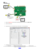
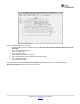
Basic Operation 1. Connect a low noise 3.3 V power supply to the VCC SMA connector. If there is no jumper between VccSMA and VccAUXPlane, either install a jumper or connect a 3.3VDC supply to the VCCAux SMA Connector located at the top left of the board. 2. Connect a low noise reference clock source (122.88 MHz for the XTAL option or 61.
1 Power Supply 3.3 V Power Power Cable Cable Vcc uWire header CLKin0 CLKin0* 3 Laptop Laptop or or PC PC Please Please See See Appendix Appendix G G for for quick quick start start on on interfacing interfacing the the board board 2 Reference clock from signal generator or other external source. 122.88 MHz (Default) Signal Generator 3. Please see Appendix D for quick start on interfacing the board. Connect PC to the uWire header. 4. Start CodeLoader4.exe 5.
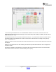
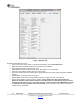
***The clock outputs tab allows the user to Enable/Disable individual clock channels, select the clock mode (Bypass/Divided/ Delayed/ Divided & Delayed), set the channel delay value (if Delay is enabled), and the channel divider value (2,4,6,…,510). This tab also allows the user to select the VCO Divider value (2,3,…,8). Note that the total PLL2 N divider value is composed of both the VCO Divider value and the N value shown in the blue box in the image, and is given by: NTOTAL = VCO Divider * N.
The PLL2 tab allows the user to change: VCO frequency PLL2 Phase detector frequency PLL2 R-counter value PLL2 N-counter value The frequency of the external VCXO (or XTAL oscillator). Note: This value must be entered in both the PLL1 and PLL2 tabs. PLL2 Charge pump gain PLL2 Charge pump state. Any changes made on this tab are reflected in the Clock Outputs tab. Note that the PLL2 Phase Detector polarity is fixed and cannot be changed by the user.
The PLL1 tab allows the user to change: External VCXO (or XTAL oscillator) frequency. Note: This value must be entered in both the PLL1 and PLL2 tabs. PLL1 Phase detector frequency PLL1 R-counter value PLL1 N-counter value CLKin (Reference) oscillator frequency PLL1 Phase Detector polarity (external VCXO tuning slope) PLL1 Charge pump gain PLL1 Charge pump state.
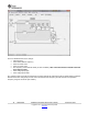
Figure 1. Bits/Pins tab. The Bits/Pins tab allows the user to: setup various clock output options. This will also be reflected on the Clock Outputs tab. Manipulate GOE and SYNC signal states (through the 10-pin header) Select internal loop filter components for PLL2 Select Reference clock functional mode: CLKin_SEL (Manual or Auto-revertive) Select the Loss-of-Signal (LOS) output type (LOS_TYPE).
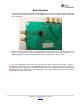
LMK040xx Board Information The LMK040xxB Evaluation Board simplifies evaluation of the LMK040xxB Precision Clock Conditioner with Dual PLLs and Integrated VCO. See Appendix H for interfacing the board. The CodeLoader software will run on a Windows 7 or Windows XP PC. The CodeLoader software is used to program the internal registers of the LMK040xxB device through a LPT or USB2ANY-uWire interface. The following block diagram illustrates the functional architecture of the LMK040xxB clock conditioner.
CLKin0 R1 N1 PLL1 CLK LE FOUT Dq2 VCO CLKin1 DATA R2 Dq1 uWire Interface N2 PLL2 CHAN DIV VCO DIV CLKout_0 D 5 Output Clock Channels LVPECL, LVDS, LVCMOS CHAN DIV D CLKout_4 Figure 3. LMK040xx with the XTAL Resonator option and Tuning Circuit LMK040xxB evaluation boards are configured with a VCXO (NSID = LMK040xxEVAL) or crystal-based oscillator circuit (NSID = LMK040xxEVAL-XO). The VCXO frequency is typically 122.88 MHz. The crystal frequency is typically 12.288 MHz.
OSCin* Copt CC1 = 2.2 nF R1 = 4.7k SMV1249-074LF R3 = 10k LMK040xx XTAL 1 nF R2 = 4.7k CC2 = 2.2 nF OSCin CPout1 Copt PLL1 Loop Filter Figure 4. XTAL Oscillator Circuit diagram November 2013 LMK040xx Evaluation Board User’s Guide Copyright © 2013, Texas Instruments Incorporated www.ti.
Below is the VCXO version of the board. VCXO 14 SNAU045A LMK040xx Evaluation Board User’s Guide Copyright © 2013, Texas Instruments Incorporated www.ti.
Below is the board with crystal installed. The surface mount crystal is installed on the bottom side of the board, along with the other components of the oscillator. Table below lists the clock output / frequency options for the LMK04000 Family. The second digit indicates VCO frequency, the second to last digit indicates output configuration. The highlighted boards indicate for which parts evaluation boards are available. Table 1.
Evaluation Board Kit Contents The evaluation board is typically shipped with a parallel port cable that is used to interconnect the board to a PC USB or LPT port, enabling the board to be programmed. The kit may also include one or more BALUN boards. Each BALUN board is configured to accept a differential signal input and provide a single-ended signal output. This enables the differential clock outputs of the LMK040xxB to be connected to test equipment or to drive single-ended circuits.
XTAL OSC Option PLL 1 Loop Filter Supply Voltage 3.3 Volts VCO Gain 10 MHz/Volt Loop Filter Components C1 = 0 C2 = 6.8 nF R2 = 2.7k ohms C3 = 100 pF C4 = 110 pF R3 = 0.6k ohms R4 = 0.2k ohms Note: PLL Loop Bandwidth is a function of K, Kvco, N as well as loop components. Changing K and N will change the loop bandwidth. PLL1 and PLL2 Parameters for VCXO Option, 100 MHz.
61.44 MHz VCXO PLL 2 Loop Filter Phase Margin 74º Loop Bandwidth 185 kHz Fcomp 61.44 MHz VCXO Frequency 61.44MHz (From PLL1) Output Frequency 1474.56 MHz Supply Voltage 3.3 Volts VCO Gain 10 MHz/Volt Loop Filter Components C1 = 0 C2 = 12 nF R2 = 1.8 k ohms C3 = 50 pF C4 = 10 pF R3 = 0.6k ohms R4 = 0.2k ohms 1600 uA Note: PLL Loop Bandwidth is a function of K, Kvco, N as well as loop components. Changing K and N will change the loop bandwidth. Table 2.
Connector Name Fout Input/Output Output Vcc Input VccAux Input CLKin0/CLKin0*, CLKin1/CLKin1* Input LOS0, LOS1 OSCin/OSCin* Output Input Vtune1 Output Vtune2 Output uWire Input/Output November 2013 Description When enabled, buffered VCO output. AC-coupled. The default configuration on the board contains a 3-dB attenuator on the Fout signal. DC power supply for the LMK040XX device. Note: The LMK040XX family contains internal voltage regulators for the VCO, PLL and related circuitry.
Connector Name LD_TP 20 Input/Output Output SNAU045A Description Test point attached to the LD pin of the device. The LD pin is attached to a multiplexer inside the device and may be programmed with a variety of internal signals for monitoring internal device functions and troubleshooting. See data sheet for further explanation. The lock detect signal is accessible through this pin. LMK040xx Evaluation Board User’s Guide Copyright © 2013, Texas Instruments Incorporated www.ti.
Typical Phase Noise Performance The following table lists the test conditions used for the phase noise measurements for the crystal oscillator option: Table 4 . LMK040XX test conditions, XTAL Oscillator Option Parameter Value PLL1 Reference clock input CLKin0*, single-ended, CLKin0 AC-coupled to GND PLL1 Reference Clock frequency 122.88 MHz PLL1 Phase detector frequency 1024 kHz PLL1 Charge Pump Gain 100 uA VCXO frequency 12.288 MHz, Ecliptek ECX-6465 PLL2 phase detector frequency 12.
LMK040x1 Evaluation Board VCXO Phase Noise -80 61.44MHz VCXO 100MHz VCXO -90 -100 dBc -110 -120 -130 -140 -150 -160 100 1000 10000 100000 1000000 10000000 100000000 Offset (Hz) Figure 6. LMK040X1 Evaluation Board, typical VCXO Phase Noise, 100 MHz and 61.44 MHz VCXOs. The following table lists the test conditions used for the phase noise measurements based upon the VCXO option, 100 MHz: Table 5.
Typical Phase Noise, LMK040X1, VCXO Option -80 Fout, 1500 MHz, jitter = 193 fs LVDS, 250 MHz, jitter = 215 fs -90 LVPECL, 250 MHz, jitter = 203 fs LVCMOS, 250 MHz, jitter = 201 fs -100 dBc -110 -120 -130 -140 -150 -160 -170 100 1000 10000 100000 1000000 10000000 100000000 Offset (Hz) Figure 7. Typical Phase Noise, LMK040X1, VCXO Option (100 MHz). Jitter metrics are for an integration bandwidth of 100 Hz to 20 MHz.
Typical Phase Noise, LMK040X0, VCXO Option (61.44 MHz) -70 -80 Fout, 1.288 MHz, jitter = 255 fs -90 LVCMOS, 153.6 MHz, jitter = 250 fs LVPECL, 153.6 MHz, jitter= 259 fs LVDS, 153.6 MHz, Jitter = 274 fs -100 dBc -110 -120 -130 -140 -150 -160 -170 100 1000 10000 100000 1000000 10000000 100000000 Offset (Hz) Figure 8. Typical Phase noise, LMK04020, VCXO Option (61.44 MHz). Jitter metrics are for an integration bandwidth of 100 Hz to 20 MHz.
Appendix A: Schematics November 2013 LMK040xx Evaluation Board User’s Guide Copyright © 2013, Texas Instruments Incorporated www.ti.
SNAU045A LMK040xx Evaluation Board User’s Guide Copyright © 2013, Texas Instruments Incorporated www.ti.
November 2013 LMK040xx Evaluation Board User’s Guide Copyright © 2013, Texas Instruments Incorporated www.ti.
Appendix B: Board Layers Stackup Layers of the 6 layer evaluation board include: Blue is dielectrics Top to bottom layer order: LMK04000.GTL (1) LMK04000.GP1 (2) gnd LMK04000.GP2 (3) vcc LMK04000.GP3 (4) gnd LMK04000.G1 (5) vcc LMK04000.GBL (6) Top Copper. 1oz thick [LMK04000.GTL] RO4003 (Er = 3.38) CONTROLLED THICKNESS of 16 mils thick GND plane [LMK04000.GP1] FR4 (Er = ~4.6) CONTROLLED THICKNESS: 2.5 mils thick VccCLK plane [LMK04000.
Appendix C: Bill of Materials Part Capacitors 100 pF Manufacturer Part Number Qnt Identifier Kemet C0603C101J5GAC 4 100 pF 1 nF 1 nF 2.2 nF 5.6 nF 12 nF 0.1 uF Kemet Kemet Kemet Kemet Kemet Kemet Kemet C0603C101J5GAC C0603C102J5GAC C0603C102J5GAC C0603C222K5RAC C1210C562J1GAC ECH-U01123JX5 C0603C104J3RAC 14 1 1 2 1 1 10 0.
0 ohm 18 ohm 51 ohm 100 ohm 120 ohm 180 ohm 270 ohm 820 ohm 1.8 k 2.2 k 15 k 27 k 39 k 47 k 390 k Other SMV1249 3.3 V zener SMA_FRAME HEADER_2X3 HEADER_2X4 HEADER_2X5 (POLARIZED) Green LED Red LED SMA CVPD-920-100.000 0.
Open Open - 603 45 Open Open Open Open Open Open Open Open Open Open Open Open - Open 805 Open Open Open Open Open Open Open Open Open Open 93 3 4 1 1 2 3 1 2 5 1 2 November 2013 LMK040xx Evaluation Board User’s Guide Copyright © 2013, Texas Instruments Incorporated www.ti.
Appendix D: Typical BALUN Board Frequency Response The following figure illustrates the typical frequency response of BALUN using either of the MiniCircuits models listed. Typical Insertion Loss, Balun boards 0 ADT2 - 1T -1 ADTL2 - 18 -2 -3 dB -4 -5 -6 -7 -8 -9 -10 10 100 1000 10000 Hz Figure 9. Typical BALUN Frequency Response 32 SNAU045A LMK040xx Evaluation Board User’s Guide Copyright © 2013, Texas Instruments Incorporated www.ti.
Appendix E: Changing Active On-board Oscillator for PLL1 Changing from Crystal Resonator to VCXO If the board has been setup to use the crystal-based oscillator with PLL1, the crystal may be disabled and the VCXO enabled as described on the following pages: 1. Install a zero Ohm resistor in R79 (near the VCXO) November 2013 LMK040xx Evaluation Board User’s Guide Copyright © 2013, Texas Instruments Incorporated www.ti.
2. Remove resistors R62 and R63 and install 0.1 uF capacitors in C43 and C77. 3. Remove resistors R141 and R80. Install a zero Ohm resistor in R142 34 SNAU045A LMK040xx Evaluation Board User’s Guide Copyright © 2013, Texas Instruments Incorporated www.ti.
4. Install a 0 Ohm resistor in R83 and remove the 0 Ohm resistor in R85 5. Power to the VCXO is provided by placing a jumper on the Vcc_TP header across the traces labeled “VccSMA” and “VccAUXPlane”. jumper Changing from VCXO to Crystal Resonator If the board has been setup to use the VCXO for PLL1, the VCXO may be disabled and the crystal enabled as described on the following pages: November 2013 LMK040xx Evaluation Board User’s Guide Copyright © 2013, Texas Instruments Incorporated www.ti.
1. Remove the zero Ohm resistor R79 (near the VCXO) 2. Install 0 Ohm resistors R62 and R63 and remove the 0.1 uF capacitors in C43 and C77. 36 SNAU045A LMK040xx Evaluation Board User’s Guide Copyright © 2013, Texas Instruments Incorporated www.ti.
3. Install a 0 Ohm resistor at R141 and R80. Remove the zero Ohm resistor in R142 4. Remove the 0 Ohm resistor installed in R83 and install a 0 Ohm resistor in R85. November 2013 LMK040xx Evaluation Board User’s Guide Copyright © 2013, Texas Instruments Incorporated www.ti.
5. Disconnect power to the VCXO by removing the jumper on the Vcc_TP header across the traces labeled “VccSMA” and “VccAUXPlane”, if installed. jumper 38 SNAU045A LMK040xx Evaluation Board User’s Guide Copyright © 2013, Texas Instruments Incorporated www.ti.
Appendix F: Quick Start for EVM Communication Codeloader is the software used to communicate with the EVM (Please download the latest version from TI.com - http://www.ti.com/tool/codeloader). This EVM can be controlled through the uWire interface on board. There are two options in communicating with the uWire interface from the computer. OPTION 1 Open Codeloader.
The Adapter Board This table describes the pins configuration on the adapter board for each EVM board (See examples below table) Jumper Bank Code Loader Configuration EVM A B C D E F G H LMX2581 A4 B1 C2 E5 F1 G1 H1 BUFEN (pin 1), Trigger (pin 7) LMX2541 A4 C3 E4 F1 G1 H1 CE (pin 1), Trigger (pin 10) LMK0400x A0 C3 E5 F1 G1 H1 GOE (pin 7) LMK01000 A0 C1 E5 F1 G1 H1 GOE (pin 7) LMK030xx A0 C1 E5 F1 G1 H1 SYNC (pin 7) LMK02000 A0 C1 E5 F1 G1 H1 SYNC (pin 7) LMK0480x A0 B2 C3 E5 F0 G0 H1 Status_CLKin1 (pin 3)
EVALUATION BOARD/KIT/MODULE (EVM) ADDITIONAL TERMS Texas Instruments (TI) provides the enclosed Evaluation Board/Kit/Module (EVM) under the following conditions: The user assumes all responsibility and liability for proper and safe handling of the goods. Further, the user indemnifies TI from all claims arising from the handling or use of the goods.
FCC Interference Statement for Class B EVM devices This equipment has been tested and found to comply with the limits for a Class B digital device, pursuant to part 15 of the FCC Rules. These limits are designed to provide reasonable protection against harmful interference in a residential installation. This equipment generates, uses and can radiate radio frequency energy and, if not installed and used in accordance with the instructions, may cause harmful interference to radio communications.
【Important Notice for Users of EVMs for RF Products in Japan】 】 This development kit is NOT certified as Confirming to Technical Regulations of Radio Law of Japan If you use this product in Japan, you are required by Radio Law of Japan to follow the instructions below with respect to this product: 1. 2. 3. Use this product in a shielded room or any other test facility as defined in the notification #173 issued by Ministry of Internal Affairs and Communications on March 28, 2006, based on Sub-section 1.
EVALUATION BOARD/KIT/MODULE (EVM) WARNINGS, RESTRICTIONS AND DISCLAIMERS For Feasibility Evaluation Only, in Laboratory/Development Environments. Unless otherwise indicated, this EVM is not a finished electrical equipment and not intended for consumer use.
IMPORTANT NOTICE Texas Instruments Incorporated and its subsidiaries (TI) reserve the right to make corrections, enhancements, improvements and other changes to its semiconductor products and services per JESD46, latest issue, and to discontinue any product or service per JESD48, latest issue. Buyers should obtain the latest relevant information before placing orders and should verify that such information is current and complete.