L M K 0 4 1 X X - R E V 3 E V A L U A T I O N B O A R D O P E R A T I N G I N S T R U C T I O N S LMK041xx Family Precision Clock Conditioner with Dual PLLs and Integrated VCO Evaluation Board Operating Instructions 2012-01-16 LMK04100EVAL LMK04131EVAL LMK04102EVAL LMK04133EVAL Texas Instruments Precision Timing Devices 1 SNLU099
L M K 0 4 1 X X - R E V 3 E V A L U A T I O N B O A R D O P E R A T I N G I N S T R U C T I O N S Table of Contents QUICK START................................................................................................................................... 3 PLL LOOP FILTERS AND LOOP PARAMETERS ................................................................................... 4 PLL 1 Loop Filter .........................................................................................................
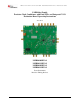
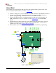
L M K 0 4 1 X X - R E V 3 E V A L U A T I O N B O A R D O P E R A T I N G I N S T R U C T I O N S Quick Start Full evaluation board instructions with data are downloadable from the product folder of the device at National Semiconductor‟s website, www.ti.com. CLKout1 CLKout1* CLKout2 CLKout2* CLKout3 Power 3.
L M K 0 4 1 X X - R E V 3 E V A L U A T I O N B O A R D O P E R A T I N G I N S T R U C T I O N S PLL Loop Filters and Loop Parameters The loop filters on the LMK041xx evaluation board are setup using the approach above. The loop filter for PLL1 has been configured for a narrow loop bandwidth (< 100 Hz), while the loop filter of PLL2 has been configured for a wide loop bandwidth (> 100 kHz). The specific loop bandwidth values depend on the phase noise performance of the oscillator mounted on the board.
L M K 0 4 1 X X - R E V 3 E V A L U A T I O N B O A R D O P E R A T I N G I N S T R U C T I O N S Evaluation Board Inputs/Outputs The following table contains descriptions of the various inputs and outputs for the evaluation board. Table 2. LMK041xx Evaluation Board I/O Connector Name CLKout0 / CLKout0*, CLKout1 / CLKout1*, CLKout2 / CLKout2*, CLKout3 / CLKout3*, CLKout4 / CLKout4* Input/Output Description Populated connectors. Differential clock output pairs. See Error! Reference source not found.
L M K 0 4 1 X X - R E V 3 Connector Name E V A L U A T I O N B O A R D O P E R A T I N G I N S T R U C T I O N S Input/Output Description Populated connectors. Reference clock inputs for PLL1. The default board configuration is setup for a single-ended reference source at CLKin0* (CLKin0 pin is AC-coupled to ground). The mode of the clock input buffer is programmable in CodeLoader on the Bits/Pins tab, and may be either bipolar junction mode or MOS mode.
L M K 0 4 1 X X - R E V 3 Connector Name Vtune1 E V A L U A T I O N B O A R D O P E R A T I N G I N S T R U C T I O N S Input/Output Description Unpopulated connector. Output Tuning voltage output from the loop filter for PLL1. If an external VCXO is used, this tuning voltage should be connected to the voltage control pin of the external VCXO. Note: Resistor R38 must be populated with a zero ohm resistor to control an off-board VCXO. Populated connector.
L M K 0 4 1 X X - R E V 3 E V A L U A T I O N B O A R D O P E R A T I N G I N S T R U C T I O N S Appendix A: CodeLoader Usage Code Loader is used to program the evaluation board with either an LPT port using the included CodeLoader cable or with a USB port using the optional USB <--> uWire cable available from http://www.ti.com/tool/usb2uwire-iface. The part number is USB2UWIRE-IFACE.
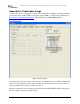
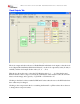
L M K 0 4 1 X X - R E V 3 E V A L U A T I O N B O A R D O P E R A T I N G I N S T R U C T I O N S Clock Outputs Tab Figure 3 - Clock Outputs tab The clock outputs tab allows the user to Enable/Disable individual clock outputs, select the clock mode (Bypass/Divided/Delayed/Divided & Delayed), set the clock output delay value (if delay is enabled), and the clock output divider value (2, 4, 6, …, 510). This tab also allows the user to select the VCO Divider value (2, 3, …, 8).
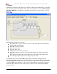
L M K 0 4 1 X X - R E V 3 E V A L U A T I O N B O A R D O P E R A T I N G I N S T R U C T I O N S The Reference Oscillator value field may be changed in either the Clock Outputs tab or the PLL2 tab. Note this value should match the value of the on-board VCXO or Crystal. When using the EN_PLL2_REF2X = 1, then Reference Oscillator field should be twice the VCXO or Crystal frequency. PLL1 Tab Figure 4 - PLL1 tab. The PLL1 tab allows the user to change: External VCXO (or Crystal oscillator) frequency.
L M K 0 4 1 X X - R E V 3 E V A L U A T I O N B O A R D O P E R A T I N G I N S T R U C T I O N S PLL2 Tab Figure 5 - PLL2 tab. The PLL2 tab allows the user to change: VCO frequency PLL2 Phase detector frequency PLL2 R-counter value PLL2 N-counter value The frequency of the external VCXO (or XTAL oscillator). Note: This value must be entered in both the PLL1 and PLL2 tabs. PLL2 Charge pump gain PLL2 Charge pump state Any changes made on this tab are reflected in the Clock Outputs tab.
L M K 0 4 1 X X - R E V 3 E V A L U A T I O N B O A R D O P E R A T I N G I N S T R U C T I O N S Bits/Pins Tab Figure 6 - Bits/Pins tab. The Bits/Pins tab allows the user to program bits directly. Many of which are not available on other tabs. Refer to the datasheet for more detailed information. The bits available are: Common Box o RESET - Set the reset bit. This will reset the device. In a normal application it is not necessary to program this bit clear since it is auto-clearing.
L M K 0 4 1 X X - R E V 3 E V A L U A T I O N B O A R D O P E R A T I N G I N S T R U C T I O N S o EN_PLL2_XTAL – Enables Crystal mode for PLL2. For use with Crystals as opposed to a VCXO. o EN_PLL2_REF2X – Doubles the reference frequency of PLL2. Note with this is enabled, the PLL_R value is invalid. Program the Reference Oscillator on PLL2 Tab to be twice the VCO frequency on PLL1 tab. This adjustment must be done manually.
L M K 0 4 1 X X - R E V 3 E V A L U A T I O N B O A R D O P E R A T I N G I N S T R U C T I O N S o SYNC* – Set high or low voltage on SYNC* pin. Checked is high voltage. If SYNC* is low, then no clock outputs will be observed on divided clock outputs! o TRIGGER – Set high or low voltage on pin 10 of uWire header. Registers Tab The registers tab shows the value of each register.
L M K 0 4 1 X X - R E V 3 E V A L U A T I O N B O A R D O P E R A T I N G I N S T R U C T I O N S Appendix B: Typical Phase Noise Performance Plots PLL1 The LMK041xx‟s two stage jitter cleaning process involves masking the reference noise with a VCXO or Crystal. Therefore the phase noise performance of the VCXO or Crystal of PLL1 is a very important contributor to the final phase noise of the system. Crystek 122.
L M K 0 4 1 X X - R E V 3 E V A L U A T I O N B O A R D O P E R A T I N G I N S T R U C T I O N S PLL2 The closed loop performance of the system as measured at the VCO output Fout. Fout phase noise performance of the various LMK options is plotted in Figure 8. Table 5 and Table 6 summarize the phase noise and jitter of Fout.
L M K 0 4 1 X X - R E V 3 E V A L U A T I O N B O A R D O P E R A T I N G I N S T R U C T I O N S Clock Outputs The LMK04100 Family features LVDS, LVPECL, 2VPECL, and LVCMOS types of outputs. Included below are various phase noise measurements for each output.
L M K 0 4 1 X X - R E V 3 E V A L U A T I O N B O A R D O P E R A T I N G I N S T R U C T I O N S LMK041x0 Phase Noise Fout LVPECL 2VPECL LVCMOS LVPECL; div4 2VPECL; div4 LVCMOS; div4 -50 -60 -70 -80 -90 -100 -110 -120 -130 -140 -150 -160 -170 10 100 1000 10000 100000 1000000 1E+07 1E+08 Offset (Hz) Figure 9 - LMK041x0B Phase Noise The Fout frequency is 1228.8 MHz. The clock out frequency is 614.4 MHz, and the clock out div 4 frequency is 153.6 MHz.
L M K 0 4 1 X X - R E V 3 E V A L U A T I O N B O A R D O P E R A T I N G I N S T R U C T I O N S LMK041x1 Phase Noise LMK040x1 Phase Noise Fout LVDS LVPECL -50 -60 -70 -80 -90 -100 -110 -120 -130 -140 -150 -160 -170 2VPECL LVCMOS LVDS; div4 LVPECL; div4 2VPECL; div4 LVCMOS; div4 10 100 1000 10000 100000 1000000 1000000 1E+08 0 Offset (Hz) Figure 10 - LMK041x1 Phase Noise The Fout frequency is 1474.56 MHz. The clock out frequency is 737.28 MHz, and the clock out div 4 frequency is 184.
L M K 0 4 1 X X - R E V 3 E V A L U A T I O N B O A R D O P E R A T I N G I N S T R U C T I O N S LMK041x2 Phase Noise Fout LMK040x2 Phase Noise LVPECL 2VPECL -50 -60 -70 -80 -90 -100 -110 -120 -130 -140 -150 -160 -170 LVCMOS LVPECL; div4 2VPECL; div4 LVCMOS; div4 10 100 1000 10000 100000 Offset (Hz) 1000000 1000000 0 1E+08 The Fout frequency is 1720.32 MHz. The clock out frequency is 860.16 MHz, and the clock out div 4 frequency is 215.04 MHz.
L M K 0 4 1 X X - R E V 3 E V A L U A T I O N B O A R D O P E R A T I N G I N S T R U C T I O N S LMK041x3 Phase Noise LMK040x3 Phase Noise -50 -60 -70 -80 -90 -100 -110 -120 -130 -140 -150 -160 -170 Fout LVDS LVPECL 2VPECL LVCMOS LVDS; div4 LVPECL; div4 2VPECL; div4 LVCMOS; div4 10 100 1000 10000 100000 1000000 1E+07 1E+08 Offset (Hz) The Fout frequency is 1966.08 MHz. The clock out frequency is 983.04 MHz, and the clock out div 4 frequency is 245.76 MHz.
GND_TP VccAuxPlane VccAuxPlane 8 7 22 SNLU099 6 PCB of bottom on placed are 200 to equal and than greater Designators 4 2 1 3 5 VccPLLPlane 4 3 VccCLKoutPlane VccCLKoutPlane 6 5 VccPLLPlane Vcc Vcc values Component LP5900 D N G 2 1 3 Open Header GND Header Vcc Open Open 2 C223 Open C221 5 1 Open R215 V_LM5900 VccAuxPlane uF 10 C21 boards Oscillator external for Off Take Power VccAuxPlane nF 3.
Attenuation and Matching 23 ohm 0 C62 R64 Open uF 0.1 C61 R63 Open uF 0.1 R62 ohm 0 XO CLKin1 SMA CLKin1 Open R60 C60 C59 C57 Open C56 Open Open Open R59 Open R58 SNLU099 R57 R56 Open 1 6 Open Vtune s V C55 Open Open R55 R54 R53 R52 VccAuxPlane VccAuxPlane D N G F R C 2 5 N RF* C54 3 4 ohm 100 3 U Open Open Open R51 Open R50 R49 R48 C52 SMA ohm 0 CLKin1* R47 ohm 0 C51 Open uF 0.
mask. metal via CMOS or LVPECL made be can CLKout3 and CLKout2 CLKout1, 3. PCB of bottom on placed are 200 to equal and than greater Designators CMOS. never and type same the both are CLKout4 and CLKout0 2. loading. capacitive of effects the test to connectors SMA CLKout all near placed be will stub A 1.
L M K 0 4 1 X X - R E V 3 E V A L U A T I O N B O A R D O P E R A T I N G I N S T R U C T I O N S Appendix D: Board Layers Stackup Layers of the 6 layer evaluation board include: Blue is dielectrics Top Copper. 1oz thick [LMK04100.GTL] Top layer for high priority high frequency signals o 1 oz CU RO4003 Dielectric, 16 mils Ground plane FR4, 2.5 mils thick.
L M K 0 4 1 X X - R E V 3 E V A L U A T I O N B O A R D O P E R A T I N G I N S T R U C T I O N S Appendix E: Bill of Materials Common Bill of Materials for Evaluation Boards (page 1/3) Part Capacitors 2.0 pF 33 pF 100 pF 1 nF 2.2 nF 6.8 nF 10 nF 12 nF Manufacturer Part Number Kemet Kemet Kemet Kemet Kemet Kemet Kemet Panasonic C0603C209C5GAC C0402C330J5GAC C0603C101J5GAC C0603C102J5GAC C0603C222K5RAC C0603C682K1RACTU C0603C103K1RACTU ECH-U01123JX5 2 3 2 1 2 1 4 1 0.
L M K 0 4 1 X X - R E V 3 E V A L U A T I O N B O A R D O P E R A T I N G I N S T R U C T I O N S Common Bill of Materials for Evaluation Boards (continued, 2/3) Resistors 0 ohm Vishay/Dale CRCW06030000Z0EA 23 18 ohm 51 ohm 100 ohm 120 ohm 180 ohm 270 ohm 1.8 k 2.2 k 2.7 k 3.9 k 4.
L M K 0 4 1 X X - R E V 3 E V A L U A T I O N B O A R D O P E R A T I N G I N S T R U C T I O N S Common Bill of Materials for Evaluation Boards (continued, 3/3) Open Open R 78 Open C 44 Open U 4 Open SMA 12 Open Open Y D 1 3 28 SNLU099 R14, R17, R21, R22, R24, R25, R27, R33, R34, R38, R42, R43, R46, R48, R49, R50, R52, R53, R54, R55, R56, R57, R58, R59, R61, R63, R64, R66, R67, R69, R70, R72, R75, R77, R78, R79, R83, R84, R86, R87, R88, R89, R90, R93, R94, R97, R98, R99, R100, R101,
L M K 0 4 1 X X - R E V 3 E V A L U A T I O N B O A R D O P E R A T I N G I N S T R U C T I O N S Bill of Material Custom to LMK04100BEVAL Part Capacitors 0.1 uF Manufacturer Part Number Kemet C0603C104J3RAC 2 C31, C42 Resistors 0 ohm 120 ohm Vishay/Dale Vishay/Dale CRCW06030000Z0EA CRCW0603120RJNEA 2 4 R9, R39 R74, R76, R80, R81 Other LMK04100B CVHD-950-122.88 National Semiconductor Crystek LMK04100B CVHD-950-122.
L M K 0 4 1 X X - R E V 3 E V A L U A T I O N B O A R D O P E R A T I N G I N S T R U C T I O N S Bill of Material Custom to LMK04131BEVAL Part Capacitors 0.1 uF Manufacturer Part Number Qnt Identifier Kemet C0603C104J3RAC 2 C31, C43 Resistors 0 ohm 120 ohm Vishay/Dale Vishay/Dale CRCW06030000Z0EA CRCW0603120RJNEA 2 2 R9, R39 R92, R95 Other LMK04131B CVHD-950-122.88 National Semiconductor Crystek LMK04131B CVHD-950-122.
L M K 0 4 1 X X - R E V 3 E V A L U A T I O N B O A R D O P E R A T I N G I N S T R U C T I O N S Bill of Material Custom to LMK04102BEVAL Part Capacitors 0.1 uF Manufacturer Part Number Kemet C0603C104J3RAC 2 C31, C42 Resistors 0 ohm 120 ohm Vishay/Dale Vishay/Dale CRCW06030000Z0EA CRCW0603120RJNEA 2 4 R9, R39 R74, R76, R80, R81 Other LMK04102B CVHD-950-122.88 National Semiconductor Crystek LMK04102B CVHD-950-122.
L M K 0 4 1 X X - R E V 3 E V A L U A T I O N B O A R D O P E R A T I N G I N S T R U C T I O N S Appendix F: Balun Information Typical Balun Frequency Response The following figure illustrates the typical frequency response of the Mini-circuit‟s ADT2-1T balun.
L M K 0 4 1 X X - R E V 3 E V A L U A T I O N B O A R D O P E R A T I N G I N S T R U C T I O N S Appendix G: VCXO/Crystal changes This appendix contains instructions for changing the active on-board oscillator for PLL1. Changing from Crystal Resonator to VCXO If the board has been setup to use the crystal-based oscillator with PLL1, the crystal may be disabled and the VCXO enabled as described on the following pages: Summary 1. Connect power to VCXO 2.
L M K 0 4 1 X X - R E V 3 E V A L U A T I O N B O A R D O P E R A T I N G I N S T R U C T I O N S 2. Disconnect Crystal RF path and connect VCXO RF path a. Remove resistors R15 and R31. b. Install 0.1 uF capacitors in C31 and C43. Figure 13 3. Connect charge pump output from PLL1 to VCXO Loop Filter (A1) and VCXO. a. Remove R37 and install a 0 ohm resistor in R39. This resistor can be “switched” between the two footprints.
L M K 0 4 1 X X - R E V 3 E V A L U A T I O N B O A R D O P E R A T I N G I N S T R U C T I O N S 4. Connect charge pump output from PLL2 to VCXO Loop filter (A2). a. Remove R10 and install a 0 ohm resistor in R9. This resistor can be “switched” between the two footprints.
L M K 0 4 1 X X - R E V 3 E V A L U A T I O N B O A R D O P E R A T I N G I N S T R U C T I O N S Changing from VCXO to Crystal Resonator If the board has been setup to use the VCXO for PLL1, the VCXO may be disabled and the crystal enabled as described on the following pages: Summary 1. Remove power from VCXO 2. Disconnect VCXO RF path and connect Crystal RF path 3. Connect charge pump output from PLL1 to Crystal Loop Filter (B1) and Crystal 4.
L M K 0 4 1 X X - R E V 3 E V A L U A T I O N B O A R D O P E R A T I N G I N S T R U C T I O N S 2. Disconnect VCXO RF path and connect Crystal RF path a. Install 0 ohm resistors R15 and R31. b. Remove 0.1 uF capacitors in C31 and C43. Figure 17 3. Connect charge pump output from PLL1 to Crystal Loop Filter (B1) and Crystal a. Remove R39 and install a 0 ohm resistor in R37. This resistor can be “switched” between the two footprints.
L M K 0 4 1 X X - R E V 3 E V A L U A T I O N B O A R D O P E R A T I N G I N S T R U C T I O N S 4. Connect charge pump output from PLL2 to Crystal Loop filter (B2) a. Remove R9 and install a 0 ohm resistor in R10. This resistor can be “switched” between the two footprints.
L M K 0 4 1 X X - R E V 3 E V A L U A T I O N B O A R D O P E R A T I N G I N S T R U C T I O N S Appendix H: LMK04100 The block diagram in Figure 20 illustrates the functional architecture of the LMK041xx clock conditioner. It features a cascaded, dual PLL arrangement, available internal loop filter components for PLL2, internal VCO with PLL2 for frequency synthesis, and clock distribution section with individual clock output dividers and delay adjustment blocks.
L M K 0 4 1 X X - R E V 3 E V A L U A T I O N B O A R D O P E R A T I N G I N S T R U C T I O N S PLL1 has been designed to work with either an off-the-shelf VCXO package or with a userdesigned discrete implementation that employs a crystal resonator and associated tuning components. The Figure 21 shows an example of a discretely implemented VCXO using a crystal resonator.
L M K 0 4 1 X X - R E V 3 E V A L U A T I O N B O A R D O P E R A T I N G I N S T R U C T I O N S OSCin* Copt CC1 = 2.2 nF R1 = 4.7k SMV1249-074LF R3 = 10k LMK040xx XTAL 1 nF R2 = 4.7k CC2 = 2.
L M K 0 4 1 X X - R E V 3 E V A L U A T I O N B O A R D O P E R A T I N G I N S T R U C T I O N S Appendix I: Properly Configuring LPT Port When trying to solve any communications issue, it is convenient to program the POWERDOWN bit to confirm high/low current draw of the evaluation board or the PLL_MUX between “Logic Low” and “Logic High” LD output to confirm successful communications. LPT Driver Loading The parallel port must be configured for proper operation.
L M K 0 4 1 X X - R E V 3 E V A L U A T I O N B O A R D O P E R A T I N G I N S T R U C T I O N S Figure 24 - Selecting the LPT Port Correct LPT Mode If communications are not working, then it is possible the LPT port mode is set improperly. It is recommended to use the simple, Output-only mode of the LPT port. This can be set in the BIOS of the computer. Common terms for this desired parallel port mode are “Normal,” “Output,” or “AT.
L M K 0 4 1 X X - R E V 3 E V A L U A T I O N B O A R D O P E R A T I N G I N S T R U C T I O N S Appendix J: Troubleshooting Information If the evaluation board is not behaving as expected, the most likely issues are… 1) Board communication issue 2) Incorrect Programming of the device 3) Setup Error Refer to this checklist for a practical guide on identifying/exposing possible issues. 1) Confirm Communications Refer to Appendix I: Properly Configuring LPT Port to trouble shoot this item.
L M K 0 4 1 X X - R E V 3 E V A L U A T I O N B O A R D O P E R A T I N G I N S T R U C T I O N S 7) If LD pin output is low, but the frequencies are the same, it is possible that excessive leakage on Vtune pin is causing the digital lock detect to not activate. By default PLL2 waits for the digital lock detect to go high before allowing PLL2 and the integrated VCO to lock. Different VCXO models have different input leakage specifications.
IMPORTANT NOTICE Texas Instruments Incorporated and its subsidiaries (TI) reserve the right to make corrections, modifications, enhancements, improvements, and other changes to its products and services at any time and to discontinue any product or service without notice. Customers should obtain the latest relevant information before placing orders and should verify that such information is current and complete.