
Datasheet


CB 1
2
3 4
5
6
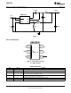
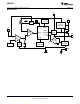
LMR14206
GND
FB
SW
PIN 1 ID
V
IN
SHDN
LMR14206
VOUT
VIN
L1
D1
R1
R2
C
BOOT
C
IN
C
OUT
FB
SW
CB
GND
SHDN
V
IN
LMR14206
SNVS733D –OCTOBER 2011–REVISED APRIL 2013
www.ti.com
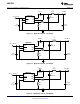
Figure 1.
Connection Diagram
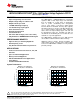
Figure 2. 6-Pin SOT (Top View)
See DDC Package
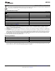
PIN DESCRIPTIONS
Pin Name Function
1 CB SW FET gate bias voltage. Connect C
BOOT
cap between CB and SW.
2 GND Ground connection.
Feedback pin: Set feedback voltage divider ratio with V
OUT
= V
FB
(1+(R1/R2)). Resistors should be
3 FB
in the 100-10K range to avoid input bias errors.
4 SHDN Logic level shutdown input. Pull to GND to disable the device and pull high to enable the device. If
this function is not used tie to V
IN
or leave open.
5 V
IN
Power input voltage pin: 4.5V to 42V normal operating range.
6 SW Power FET output: Connect to inductor, diode, and C
BOOT
cap.
2 Submit Documentation Feedback Copyright © 2011–2013, Texas Instruments Incorporated
Product Folder Links: LMR14206