
Datasheet
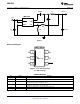


FB
GND
SW
CB
SHDN
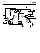
LMR14206
5V OUT
7V to 42V IN
L1
D1
60V 1A
R1
R2
5.62k
1.02k
V
IN
C
IN
C
BOOT
C
OUT
47 PF
15 PH
2.2 PF
0.15 PF
FB
GND
SW
CB
SHDN
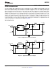
LMR14206
3.3V OUT
4.5V to 42V IN
L1
D1
60V 1A
R1
R2
3.4k
1.02k
V
IN
C
IN
C
BOOT
C
OUT
47 PF
15 PH
0.15 PF
2.2 PF
LMR14206
www.ti.com
SNVS733D –OCTOBER 2011–REVISED APRIL 2013
LAYOUT CONSIDERATIONS
To reduce problems with conducted noise pick up, the ground side of the feedback network should be connected
directly to the GND pin with its own connection. The feedback network, resistors R1 and R2, should be kept
close to the FB pin, and away from the inductor to minimize coupling noise into the feedback pin. The input
bypass capacitor C
IN
must be placed close to the V
IN
pin. This will reduce copper trace resistance which effects
input voltage ripple of the IC. The inductor L1 should be placed close to the SW pin to reduce EMI and capacitive
coupling. The output capacitor, C
OUT
should be placed close to the junction of L1 and the diode D1. The L1, D1,
and C
OUT
trace should be as short as possible to reduce conducted and radiated noise and increase overall
efficiency. The ground connection for the diode, C
IN
, and C
OUT
should be as small as possible and tied to the
system ground plane in only one spot (preferably at the C
OUT
ground point) to minimize conducted noise in the
system ground plane. For more detail on switching power supply layout considerations see Application Note AN-
1149: Layout Guidelines for Switching Power Supplies SNVA021.
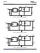
Typical Applications
Figure 9. Application Circuit, 3.3V Output
Figure 10. Application Circuit, 5V Output
Copyright © 2011–2013, Texas Instruments Incorporated Submit Documentation Feedback 9
Product Folder Links: LMR14206