LMS8117A LMS8117A 1A Low-Dropout Linear Regulator Literature Number: SNOS487E
LMS8117A 1A Low-Dropout Linear Regulator General Description Features The LMS8117A is a series of low dropout voltage regulators with a dropout of 1.2V at 1A of load current. It has the same pin-out as National Semiconductor’s industry standard LM317. The LMS8117A is available in an adjustable version, which can set the output voltage from 1.25V to 13.8V with only two external resistors. In addition, it is also available in two fixed voltages, 1.8V and 3.3V.
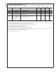
LMS8117A Ordering Information Package 3-lead SOT-223 3-lead TO-252 Temperature Range (TJ) Packaging Marking Transport Media NSC Drawing LMS8117AMP-ADJ LS0A 1k Tape and Reel MP04A LMS8117AMPX-ADJ LS0A 2k Tape and Reel LMS8117AMP-1.8 LS00 1k Tape and Reel LMS8117AMPX-1.8 LS00 2k Tape and Reel LMS8117AMP-3.3 LS01 1k Tape and Reel LMS8117AMPX-3.3 LS01 2k Tape and Reel 0˚C to +125˚C LMS8117ADT-ADJ LMS8117ADT-ADJ Rails LMS8117ADTX-ADJ LMS8117ADT-ADJ 2.
Soldering Information If Military/Aerospace specified devices are required, please contact the National Semiconductor Sales Office/ Distributors for availability and specifications. ESD Tolerance (Note 3) Infrared (20 sec) Maximum Input Voltage (VIN to GND) Operating Ratings (Note 1) LMS8117A-ADJ, LMS8117A-1.8, LMS8117A-3.3 Power Dissipation (Note 2) 235˚C 2000V Input Voltage (VIN to GND) 20V LMS8117A-ADJ, LMS8117A-1.8, LMS8117A-3.
LMS8117A Electrical Characteristics (Continued) Typicals and limits appearing in normal type apply for TJ = 25˚C. Limits appearing in Boldface type apply over the entire junction temperature range for operation, 0˚C to 125˚C. Symbol Parameter Conditions Temperature Stability Min (Note 5) Typ (Note 4) Max (Note 5) Units 0.5 % 0.3 % Long Term Stability TA = 125˚C, 1000Hrs RMS Output Noise (% of VOUT), 10Hz ≤ f ≤ 10kHz 0.
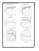
LMS8117A Typical Performance Characteristics Dropout Voltage (VIN-V OUT) Short-Circuit Current 10119623 10119622 Load Regulation LMS8117A-ADJ Ripple Rejection vs. Current 10119606 10119624 LMS8117A-ADJ Ripple Rejection Temperature Stability 10119607 10119625 5 www.national.
LMS8117A Typical Performance Characteristics (Continued) Adjust Pin Current LMS8117A-1.8 Load Transient Response 10119626 10119608 LMS8117A-3.3 Load Transient Response LMS8117A-1.8 Line Transient Response 10119610 10119609 LMS8117A-3.3 Line Transient Response 10119611 www.national.
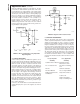
LMS8117A Application Note 1.0 EXTERNAL CAPACITORS/STABILITY 1.1 Input Bypass Capacitor An input capacitor is recommended. A 10µF tantalum on the input is a suitable input bypassing for almost all applications. 1.2 Adjust Terminal Bypass Capacitor The adjust terminal can be bypassed to ground with a bypass capacitor (CADJ) to improve ripple rejection. This bypass capacitor prevents ripple from being amplified as the output voltage is increased.
LMS8117A Application Note (Continued) When the adjustable regulator is used (Figure 3), the best performance is obtained with the positive side of the resistor R1 tied directly to the output terminal of the regulator rather than near the load. This eliminates line drops from appearing effectively in series with the reference and degrading regulation. For example, a 5V regulator with 0.05Ω resistance between the regulator and load will have a load regulation due to line resistance of 0.05Ω x IL.
LMS8117A Application Note (Continued) 10119637 FIGURE 5. Cross-sectional view of Integrated Circuit Mounted on a printed circuit board. Note that the case temperature is measured at the point where the leads contact with the mounting pad surface TR(max)=TJ(max)-TA(max) where TJ(max) is the maximum allowable junction temperature (125˚C), and TA(max) is the maximum ambient temperature which will be encountered in the application.
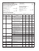
LMS8117A Application Note (Continued) TABLE 1. θJA Different Heatsink Area Layout Copper Area Thermal Resistance Top Side (in2)* Bottom Side (in2) (θJA,˚C/W) SOT-223 (θJA,˚C/W) TO-252 1 0.0123 0 136 103 2 0.066 0 123 87 3 0.3 0 84 60 4 0.53 0 75 54 5 0.76 0 69 52 47 6 1 0 66 7 0 0.2 115 84 8 0 0.4 98 70 9 0 0.6 89 63 10 0 0.8 82 57 11 0 1 79 57 12 0.066 0.066 125 89 13 0.175 0.175 93 72 14 0.284 0.284 83 61 15 0.392 0.
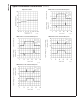
LMS8117A Application Note (Continued) 10119636 FIGURE 10. Maximum Allowable Power Dissipation vs. Ambient Temperature for TO-252 10119613 FIGURE 7. θJA vs. 1oz Copper Area for SOT-223 10119614 10119634 FIGURE 8. θJA vs. 2oz Copper Area for TO-252 FIGURE 11. Maximum Allowable Power Dissipation vs. 1oz Copper Area for SOT-223 10119635 10119612 FIGURE 12. Maximum Allowable Power Dissipation vs. 2oz Copper Area for TO-252 FIGURE 9. Maximum Allowable Power Dissipation vs.
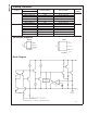
LMS8117A Application Note (Continued) 10119620 FIGURE 13. Top View of the Thermal Test Pattern in Actual Scale www.national.
LMS8117A Application Note (Continued) 10119621 FIGURE 14. Bottom View of the Thermal Test Pattern in Actual Scale 13 www.national.
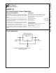
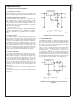
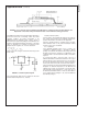
LMS8117A Typical Application Circuits 10119629 1.25V to 10V Adjustable Regulator with Improved Ripple Rejection 10119627 5V Logic Regulator with Electronic Shutdown* www.national.
LMS8117A Physical Dimensions inches (millimeters) unless otherwise noted 3-Lead SOT-223 NS Package Number MP04A 15 www.national.
LMS8117A 1A Low-Dropout Linear Regulator Physical Dimensions inches (millimeters) unless otherwise noted (Continued) 3-Lead TO-252 NS Package Number TD03B National does not assume any responsibility for use of any circuitry described, no circuit patent licenses are implied and National reserves the right at any time without notice to change said circuitry and specifications. For the most current product information visit us at www.national.com.
IMPORTANT NOTICE Texas Instruments Incorporated and its subsidiaries (TI) reserve the right to make corrections, modifications, enhancements, improvements, and other changes to its products and services at any time and to discontinue any product or service without notice. Customers should obtain the latest relevant information before placing orders and should verify that such information is current and complete.