LMV321-N, LMV321-N-Q1, LMV358-N, LMV358-N-Q1 LMV324-N, LMV324-N-Q1 www.ti.
LMV321-N, LMV321-N-Q1, LMV358-N, LMV358-N-Q1 LMV324-N, LMV324-N-Q1 SNOS012I – AUGUST 2000 – REVISED FEBRUARY 2013 www.ti.com These devices have limited built-in ESD protection. The leads should be shorted together or the device placed in conductive foam during storage or handling to prevent electrostatic damage to the MOS gates.
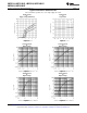
LMV321-N, LMV321-N-Q1, LMV358-N, LMV358-N-Q1 LMV324-N, LMV324-N-Q1 www.ti.com SNOS012I – AUGUST 2000 – REVISED FEBRUARY 2013 2.7V DC Electrical Characteristics Unless otherwise specified, all limits guaranteed for TJ = 25°C, V+ = 2.7V, V− = 0V, VCM = 1.0V, VO = V+/2 and RL > 1 MΩ. Symbol Parameter Conditions Min (1) Typ Max 1.
LMV321-N, LMV321-N-Q1, LMV358-N, LMV358-N-Q1 LMV324-N, LMV324-N-Q1 SNOS012I – AUGUST 2000 – REVISED FEBRUARY 2013 www.ti.com 5V DC Electrical Characteristics Unless otherwise specified, all limits guaranteed for T J = 25°C, V+ = 5V, V− = 0V, VCM = 2.0V, VO = V+/2 and R L > 1 MΩ. Boldface limits apply at the temperature extremes. Symbol Parameter Conditions Min (1) Typ Max Units 1.
LMV321-N, LMV321-N-Q1, LMV358-N, LMV358-N-Q1 LMV324-N, LMV324-N-Q1 www.ti.com SNOS012I – AUGUST 2000 – REVISED FEBRUARY 2013 5V AC Electrical Characteristics Unless otherwise specified, all limits guaranteed for TJ = 25°C, V+ = 5V, V− = 0V, VCM = 2.0V, VO = V+/2 and R L > 1 MΩ. Boldface limits apply at the temperature extremes.
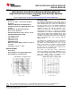
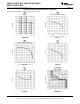
LMV321-N, LMV321-N-Q1, LMV358-N, LMV358-N-Q1 LMV324-N, LMV324-N-Q1 SNOS012I – AUGUST 2000 – REVISED FEBRUARY 2013 www.ti.com Typical Performance Characteristics Unless otherwise specified, VS = +5V, single supply, TA = 25°C. 6 Supply Current vs. Supply Voltage (LMV321-N) Input Current vs. Temperature Figure 4. Figure 5. Sourcing Current vs. Output Voltage Sourcing Current vs. Output Voltage Figure 6. Figure 7. Sinking Current vs. Output Voltage Sinking Current vs. Output Voltage Figure 8.
LMV321-N, LMV321-N-Q1, LMV358-N, LMV358-N-Q1 LMV324-N, LMV324-N-Q1 www.ti.com SNOS012I – AUGUST 2000 – REVISED FEBRUARY 2013 Typical Performance Characteristics (continued) Unless otherwise specified, VS = +5V, single supply, TA = 25°C. Output Voltage Swing vs. Supply Voltage Input Voltage Noise vs. Frequency Figure 10. Figure 11. Input Current Noise vs. Frequency Input Current Noise vs. Frequency Figure 12. Figure 13. Crosstalk Rejection vs. Frequency PSRR vs. Frequency Figure 14. Figure 15.
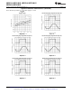
LMV321-N, LMV321-N-Q1, LMV358-N, LMV358-N-Q1 LMV324-N, LMV324-N-Q1 SNOS012I – AUGUST 2000 – REVISED FEBRUARY 2013 www.ti.com Typical Performance Characteristics (continued) Unless otherwise specified, VS = +5V, single supply, TA = 25°C. 8 CMRR vs. Frequency CMRR vs. Input Common Mode Voltage Figure 16. Figure 17. CMRR vs. Input Common Mode Voltage ΔVOS vs. CMR Figure 18. Figure 19. ΔV OS vs. CMR Input Voltage vs. Output Voltage Figure 20. Figure 21.
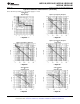
LMV321-N, LMV321-N-Q1, LMV358-N, LMV358-N-Q1 LMV324-N, LMV324-N-Q1 www.ti.com SNOS012I – AUGUST 2000 – REVISED FEBRUARY 2013 Typical Performance Characteristics (continued) Unless otherwise specified, VS = +5V, single supply, TA = 25°C. Input Voltage vs. Output Voltage Open Loop Frequency Response Figure 22. Figure 23. Open Loop Frequency Response Open Loop Frequency Response vs. Temperature Figure 24. Figure 25. Gain and Phase vs. Capacitive Load Gain and Phase vs. Capacitive Load Figure 26.
LMV321-N, LMV321-N-Q1, LMV358-N, LMV358-N-Q1 LMV324-N, LMV324-N-Q1 SNOS012I – AUGUST 2000 – REVISED FEBRUARY 2013 www.ti.com Typical Performance Characteristics (continued) Unless otherwise specified, VS = +5V, single supply, TA = 25°C. 10 Slew Rate vs. Supply Voltage Non-Inverting Large Signal Pulse Response Figure 28. Figure 29. Non-Inverting Large Signal Pulse Response Non-Inverting Large Signal Pulse Response Figure 30. Figure 31.
LMV321-N, LMV321-N-Q1, LMV358-N, LMV358-N-Q1 LMV324-N, LMV324-N-Q1 www.ti.com SNOS012I – AUGUST 2000 – REVISED FEBRUARY 2013 Typical Performance Characteristics (continued) Unless otherwise specified, VS = +5V, single supply, TA = 25°C. Non-Inverting Small Signal Pulse Response Inverting Large Signal Pulse Response Figure 34. Figure 35. Inverting Large Signal Pulse Response Inverting Large Signal Pulse Response Figure 36. Figure 37.
LMV321-N, LMV321-N-Q1, LMV358-N, LMV358-N-Q1 LMV324-N, LMV324-N-Q1 SNOS012I – AUGUST 2000 – REVISED FEBRUARY 2013 www.ti.com Typical Performance Characteristics (continued) Unless otherwise specified, VS = +5V, single supply, TA = 25°C. 12 Inverting Small Signal Pulse Response Stability vs. Capacitive Load Figure 40. Figure 41. Stability vs. Capacitive Load Stability vs. Capacitive Load Figure 42. Figure 43. Stability vs. Capacitive Load THD vs. Frequency Figure 44. Figure 45.
LMV321-N, LMV321-N-Q1, LMV358-N, LMV358-N-Q1 LMV324-N, LMV324-N-Q1 www.ti.com SNOS012I – AUGUST 2000 – REVISED FEBRUARY 2013 Typical Performance Characteristics (continued) Unless otherwise specified, VS = +5V, single supply, TA = 25°C. Open Loop Output Impedance vs. Frequency Short Circuit Current vs. Temperature (Sinking) Figure 46. Figure 47. Short Circuit Current vs. Temperature (Sourcing) Figure 48.
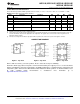
LMV321-N, LMV321-N-Q1, LMV358-N, LMV358-N-Q1 LMV324-N, LMV324-N-Q1 SNOS012I – AUGUST 2000 – REVISED FEBRUARY 2013 www.ti.com APPLICATION INFORMATION BENEFITS OF THE LMV321-N/LMV358-N/LMV324-N Size The small footprints of the LMV321-N/LMV358-N/LMV324-N packages save space on printed circuit boards, and enable the design of smaller electronic products, such as cellular phones, pagers, or other portable systems.
LMV321-N, LMV321-N-Q1, LMV358-N, LMV358-N-Q1 LMV324-N, LMV324-N-Q1 www.ti.com SNOS012I – AUGUST 2000 – REVISED FEBRUARY 2013 Figure 50. Output Swing of LM324 CAPACITIVE LOAD TOLERANCE The LMV321-N/LMV358-N/LMV324-N can directly drive 200 pF in unity-gain without oscillation. The unity-gain follower is the most sensitive configuration to capacitive loading. Direct capacitive loading reduces the phase margin of amplifiers.
LMV321-N, LMV321-N-Q1, LMV358-N, LMV358-N-Q1 LMV324-N, LMV324-N-Q1 SNOS012I – AUGUST 2000 – REVISED FEBRUARY 2013 www.ti.com Figure 53. Indirectly Driving A Capacitive Load with DC Accuracy INPUT BIAS CURRENT CANCELLATION The LMV321-N/LMV358-N/LMV324-N family has a bipolar input stage. The typical input bias current of LMV321N/LMV358-N/LMV324-N is 15 nA with 5V supply. Thus a 100 kΩ input resistor will cause 1.5 mV of error voltage.
LMV321-N, LMV321-N-Q1, LMV358-N, LMV358-N-Q1 LMV324-N, LMV324-N-Q1 www.ti.com SNOS012I – AUGUST 2000 – REVISED FEBRUARY 2013 Figure 55. Difference Amplifier Instrumentation Circuits The input impedance of the previous difference amplifier is set by the resistors R1, R2, R3, and R4. To eliminate the problems of low input impedance, one way is to use a voltage follower ahead of each input as shown in the following two instrumentation amplifiers.
LMV321-N, LMV321-N-Q1, LMV358-N, LMV358-N-Q1 LMV324-N, LMV324-N-Q1 SNOS012I – AUGUST 2000 – REVISED FEBRUARY 2013 www.ti.com Figure 57. Two-Op-Amp Instrumentation Amplifier Single-Supply Inverting Amplifier There may be cases where the input signal going into the amplifier is negative. Because the amplifier is operating in single supply voltage, a voltage divider using R3 and R4 is implemented to bias the amplifier so the input signal is within the input common-mode voltage range of the amplifier.
LMV321-N, LMV321-N-Q1, LMV358-N, LMV358-N-Q1 LMV324-N, LMV324-N-Q1 www.ti.com SNOS012I – AUGUST 2000 – REVISED FEBRUARY 2013 Figure 59. Simple Low-Pass Active Filter Figure 60. Frequency Response of Simple Low-Pass Active Filter in Figure 11 Note that the single-op-amp active filters are used in the applications that require low quality factor, Q( ≤ 10), low frequency (≤ 5 kHz), and low gain (≤ 10), or a small value for the product of gain times Q (≤ 100).
LMV321-N, LMV321-N-Q1, LMV358-N, LMV358-N-Q1 LMV324-N, LMV324-N-Q1 SNOS012I – AUGUST 2000 – REVISED FEBRUARY 2013 www.ti.com (3) Figure 61. Sallen-Key 2nd-Order Active Low-Pass Filter The following paragraphs explain how to select values for R1, R2, R3, R4, C1, and C 2 for given filter requirements, such as ALP, Q, and fc.
LMV321-N, LMV321-N-Q1, LMV358-N, LMV358-N-Q1 LMV324-N, LMV324-N-Q1 www.ti.com SNOS012I – AUGUST 2000 – REVISED FEBRUARY 2013 From Equation 2 and Equation 9, we obtain (10) (11) The values of C1 and C2 are normally close to or equal to (12) As a design example: Require: ALP = 2, Q = 1, fc = 1 kHz Start by selecting C1 and C2.
LMV321-N, LMV321-N-Q1, LMV358-N, LMV358-N-Q1 LMV324-N, LMV324-N-Q1 SNOS012I – AUGUST 2000 – REVISED FEBRUARY 2013 www.ti.com Figure 62. Sallen-Key 2nd-Order Active High-Pass Filter State Variable Filter A state variable filter requires three op amps. One convenient way to build state variable filters is with a quad op amp, such as the LMV324 (Figure 63). This circuit can simultaneously represent a low-pass filter, high-pass filter, and bandpass filter at three different outputs.
LMV321-N, LMV321-N-Q1, LMV358-N, LMV358-N-Q1 LMV324-N, LMV324-N-Q1 www.ti.com SNOS012I – AUGUST 2000 – REVISED FEBRUARY 2013 (23) where for all three filters, (24) (25) A design example for a bandpass filter is shown below: Assume the system design requires a bandpass filter with f are capacitor and resistor values. O = 1 kHz and Q = 50.
LMV321-N, LMV321-N-Q1, LMV358-N, LMV358-N-Q1 LMV324-N, LMV324-N-Q1 SNOS012I – AUGUST 2000 – REVISED FEBRUARY 2013 www.ti.com PULSE GENERATORS AND OSCILLATORS A pulse generator is shown in Figure 64. Two diodes have been used to separate the charge and discharge paths to capacitor C. Figure 64. Pulse Generator When the output voltage VO is first at its high, VOH, the capacitor C is charged toward VOH through R2.
LMV321-N, LMV321-N-Q1, LMV358-N, LMV358-N-Q1 LMV324-N, LMV324-N-Q1 www.ti.com SNOS012I – AUGUST 2000 – REVISED FEBRUARY 2013 Figure 65. Waveforms of the Circuit in Figure 16 As shown in the waveforms in Figure 65, the pulse width (T1) is set by R2, C and VOH, and the time between pulses (T2) is set by R1, C and VOL. This pulse generator can be made to have different frequencies and pulse width by selecting different capacitor value and resistor values.
LMV321-N, LMV321-N-Q1, LMV358-N, LMV358-N-Q1 LMV324-N, LMV324-N-Q1 SNOS012I – AUGUST 2000 – REVISED FEBRUARY 2013 www.ti.com Figure 67 is a squarewave generator with the same path for charging and discharging the capacitor. Figure 67. Squarewave Generator CURRENT SOURCE AND SINK The LMV321-N/LMV358-N/LMV324-N can be used in feedback loops which regulate the current in external PNP transistors to provide current sources or in external NPN transistors to provide current sinks.
LMV321-N, LMV321-N-Q1, LMV358-N, LMV358-N-Q1 LMV324-N, LMV324-N-Q1 www.ti.com SNOS012I – AUGUST 2000 – REVISED FEBRUARY 2013 High Compliance Current Sink A current sink circuit is shown in Figure 69. The circuit requires only one resistor (RE) and supplies an output current which is directly proportional to this resistor value. Figure 69. High Compliance Current Sink POWER AMPLIFIER A power amplifier is illustrated in Figure 70.
LMV321-N, LMV321-N-Q1, LMV358-N, LMV358-N-Q1 LMV324-N, LMV324-N-Q1 SNOS012I – AUGUST 2000 – REVISED FEBRUARY 2013 www.ti.com COMPARATOR WITH HYSTERESIS The LMV321-N/LMV358-N/LMV324-N can be used as a low power comparator. Figure 72 shows a comparator with hysteresis. The hysteresis is determined by the ratio of the two resistors.
LMV321-N, LMV321-N-Q1, LMV358-N, LMV358-N-Q1 LMV324-N, LMV324-N-Q1 www.ti.com SNOS012I – AUGUST 2000 – REVISED FEBRUARY 2013 REVISION HISTORY Changes from Revision H (February 2013) to Revision I • Page Changed layout of National Data Sheet to TI format ..........................................................................................................
PACKAGE OPTION ADDENDUM www.ti.
PACKAGE OPTION ADDENDUM www.ti.
PACKAGE OPTION ADDENDUM www.ti.
PACKAGE OPTION ADDENDUM www.ti.com 1-Nov-2013 (6) Lead/Ball Finish - Orderable Devices may have multiple material finish options. Finish options are separated by a vertical ruled line. Lead/Ball Finish values may wrap to two lines if the finish value exceeds the maximum column width. Important Information and Disclaimer:The information provided on this page represents TI's knowledge and belief as of the date that it is provided.
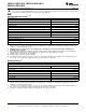
PACKAGE MATERIALS INFORMATION www.ti.com 11-Oct-2013 TAPE AND REEL INFORMATION *All dimensions are nominal Device Package Package Pins Type Drawing SPQ LMV321M5 SOT-23 LMV321M5X LMV321M7 Reel Reel A0 Diameter Width (mm) (mm) W1 (mm) 3.2 B0 (mm) K0 (mm) P1 (mm) W Pin1 (mm) Quadrant 3.2 1.4 4.0 8.0 Q3 DBV 5 1000 178.0 8.4 SOT-23 DBV 5 3000 178.0 8.4 3.2 3.2 1.4 4.0 8.0 Q3 SC70 DCK 5 1000 178.0 8.4 2.25 2.45 1.2 4.0 8.0 Q3 LMV321M7/NOPB SC70 DCK 5 1000 178.
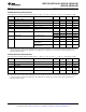
PACKAGE MATERIALS INFORMATION www.ti.com 11-Oct-2013 Device Package Package Pins Type Drawing SPQ Reel Reel A0 Diameter Width (mm) (mm) W1 (mm) B0 (mm) K0 (mm) P1 (mm) W Pin1 (mm) Quadrant LMV358MX SOIC D 8 2500 330.0 12.4 6.5 5.4 2.0 8.0 12.0 Q1 LMV358MX/NOPB SOIC D 8 2500 330.0 12.4 6.5 5.4 2.0 8.0 12.0 Q1 LMV358Q1MAX/NOPB SOIC D 8 2500 330.0 12.4 6.5 5.4 2.0 8.0 12.0 Q1 LMV358Q1MM/NOPB VSSOP DGK 8 1000 178.0 12.4 5.3 3.4 1.4 8.0 12.
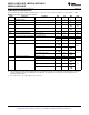
PACKAGE MATERIALS INFORMATION www.ti.com 11-Oct-2013 Device Package Type Package Drawing Pins SPQ Length (mm) Width (mm) Height (mm) LMV321Q3M5X/NOPB SOT-23 DBV 5 3000 210.0 185.0 35.0 LMV324MTX TSSOP PW 14 2500 367.0 367.0 35.0 LMV324MX SOIC D 14 2500 367.0 367.0 35.0 LMV324MX/NOPB SOIC D 14 2500 367.0 367.0 35.0 LMV324Q1MAX/NOPB SOIC D 14 2500 367.0 367.0 35.0 LMV324Q3MAX/NOPB SOIC D 14 2500 367.0 367.0 35.0 LMV358MM VSSOP DGK 8 1000 210.
IMPORTANT NOTICE Texas Instruments Incorporated and its subsidiaries (TI) reserve the right to make corrections, enhancements, improvements and other changes to its semiconductor products and services per JESD46, latest issue, and to discontinue any product or service per JESD48, latest issue. Buyers should obtain the latest relevant information before placing orders and should verify that such information is current and complete.