
Datasheet
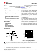
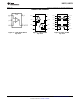


C
C1
+
V
OUT
+
-
-
C
F
V
IN
+
-
R
B1
V
+
R
B2
R
2
100 k:
R
1
1 k:
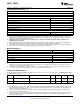
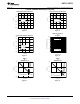
120
100
10k
10M
-40
20
GAIN (dB)
1M
100k
1k
80
60
0
-20
40
100
FREQUENCY (Hz)
PHASE
GAIN
V
S
= 5V
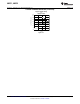
120
-40
20
80
60
0
-20
40
100
PHASE
(
°
)
LMV551, LMV552
www.ti.com
SNOSAQ5G –FEBRUARY 2007–REVISED FEBRUARY 2013
LMV551/LMV552/LMV554 3 MHz, Micropower RRO Amplifiers
Check for Samples: LMV551, LMV552
1
FEATURES
DESCRIPTION
The LMV551/LMV552/LMV554 are high performance,
2
• (Typical 5V Supply, Unless Otherwise Noted.)
low power operational amplifiers implemented with
• Guaranteed 3V and 5.0V Performance
TI’s advanced VIP50 process. They feature 3 MHz of
• High Unity Gain Bandwidth 3 MHz
bandwidth while consuming only 37 μA of current per
amplifier, which is an exceptional bandwidth to power
• Supply Current (Per Amplifier) 37 µA
ratio in this op amp class. These amplifiers are unity
• CMRR 93 dB
gain stable and provide an excellent solution for low
• PSRR 90 dB
power applications requiring a wide bandwidth.
• Slew Rate 1 V/µs
The LMV551/LMV552/LMV554 have a rail-to-rail
• Output Swing with 100 kΩ Load 70 mV From
output stage and an input common mode range that
Rail
extends below ground.
• Total Harmonic Distortion 0.003% @ 1 kHz, 2
The LMV551/LMV552/LMV554 have an operating
kΩ
supply voltage range from 2.7V to 5.5V. These
amplifiers can operate over a wide temperature range
• Temperature Range −40°C to 125°C
(−40°C to 125°C) making them a great choice for
automotive applications, sensor applications as well
APPLICATIONS
as portable instrumentation applications. The
• Active Filter
LMV551 is offered in the ultra tiny 5-Pin SC70 and 5-
Pin SOT-23 package. The LMV552 is offered in an 8-
• Portable Equipment
Pin VSSOP package. The LMV554 is offered in the
• Automotive
14-Pin TSSOP.
• Battery Powered Systems
• Sensors and Instrumentation
Typical Application
Figure . Figure 1. Open Loop Gain and Phase vs.
Frequency
These devices have limited built-in ESD protection. The leads should be shorted together or the device placed in conductive foam
during storage or handling to prevent electrostatic damage to the MOS gates.
1
Please be aware that an important notice concerning availability, standard warranty, and use in critical applications of
Texas Instruments semiconductor products and disclaimers thereto appears at the end of this data sheet.
2All trademarks are the property of their respective owners.
PRODUCTION DATA information is current as of publication date.
Copyright © 2007–2013, Texas Instruments Incorporated
Products conform to specifications per the terms of the Texas
Instruments standard warranty. Production processing does not
necessarily include testing of all parameters.