
Datasheet

RF INPUT PEAK VOLTAGE (dBVp)
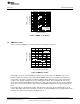
EMIRR
V_PEAK
(dB)
140
130
120
110
100
90
80
70
60
50
40
30
20
-40 -30 -20 -10 0 10
1800 MHz
900MHz
400 MHz
2400 MHz
FREQUENCY (MHz)
EMIRR
V_PEAK
(dB)
140
130
120
110
100
90
80
70
60
50
40
30
20
10 100 1000 10000
125°C
85°C
-40°C
25°C
V
+
= 3.3V, 5.0V
V
PEAK
= -20 dBVp
www.ti.com
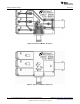
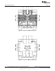
Measurement Results
Figure 1. EMIRR vs. Frequency
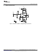
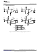
7.2 EMIRR Vs. Power
Figure 2 shows the EMIRR as a function of power at four typical frequencies.
Figure 2. EMIRR vs. Power
In this figure two areas can be distinguished. At the left side of the figure, the EMIRR increases as a
function of input level; whereas at the right side the EMIRR decreases as a function of the input level.
The left side of the figure is actually an artifact resulting from the limited accuracy of the measurement
setup. For the relatively low input levels, the resulting offset voltage shift is well below the noise level.
Thus, when calculating the EMIRR for that region, the ratio of the input level to the noise level is depicted.
As the noise level is constant for the setup, an increasing EMIRR is obtained for increasing input signal
level.
For the right side, the obtained offset-shift is well above the noise level. As the relation between offset
voltage shift and RF input level is quadratic, the ratio as used in the EMIRR is inversely proportional to the
RF input level, which is in line with the displayed slope of “−1”.
3
SNOA530A–October 2008–Revised April 2013 AN-1867 EMIRR Evaluation Boards for LMV831/LMV832/LMV834
Submit Documentation Feedback
Copyright © 2008–2013, Texas Instruments Incorporated