LMX2531LQ1515E Evaluation Board Operating Instructions National Semiconductor Corporation Timing Devices Business Group 10333 North Meridian Suite 400 Indianapolis, IN 46290 LMX2531LQ1515EFPEB Rev 4.02.
L M X 2 5 3 1 L Q 1 3 1 2 E E V A L U A T I O N B O A R D O P E R A T I N G I N S T R U C T I O N S Table of Contents TABLE OF CONTENTS ...................................................................................................................... 2 LOOP FILTER .................................................................................................................................. 3 QUICK SETUP .............................................................................................
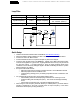
L M X 2 5 3 1 L Q 1 3 1 2 E E V A L U A T I O N B O A R D O P E R A T I N G I N S T R U C T I O N S Loop Filter Loop Bandwidth 8.1 kHz Kφ 1440 uA (16X) Phase Margin 61.2 deg Fcomp 10 MHz Crystal Frequency 10 MHz Output Frequency 1450 – 1580 MHz (DIV2=0) 725 - 790 MHz (DIV2=1) Supply Voltage 3.0 Volts VCO Gain 4 - 7 MHz/Volt CPout 20 KΩ 20 KΩ VCO 100 nF 100 pF 100 pF 1 KΩ open Vtune Quick Setup • • • • • • • • Install the CodeLoader software which is available at www.
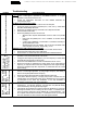
L M X 2 5 3 1 L Q 1 3 1 2 E E V A L U A T I O N B O A R D O P E R A T I N G I N S T R U C T I O N S Troubleshooting Far-out Phase noise is worse than evaluation board instructions show Close-in phase noise is worse than evaluation board instructions show Part responds to programming, but does not lock to the correct frequency Software does not communicate with the evaluation boards Problem Corrective Actions All Modes • Ensure a valid signal is presented to the OSCin connector.
Output Frequency = 1515 MHz Internal Divide by 2 Disabled (DIV2=0) Output Frequency = 757.
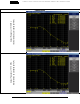
L M X 2 5 3 1 L Q 1 3 1 2 E E V A L U A T I O N B O A R D O P E R A T I N G I N S T R U C T I O N S Fout = 1470 MHz Free-Running VCO Phase Noise (Internal Divide by 2 Disabled) The plots to the left show the true phase noise capability of the VCO. In order to take these plots, the E5052 phase nose analyzer was used. The method was to lock the PLL to the Fout = 1515 MHz proper frequency, then disable the EN_PLL, EN_PLLLDO1, and EN_PLLLDO2 bits.
L M X 2 5 3 1 L Q 1 3 1 2 E E V A L U A T I O N B O A R D O P E R A T I N G I N S T R U C T I O N S Fout = 725 MHz (1450 MHz/2) Free-Running VCO Phase Noise (Internal Divide by 2 Enabled) The plots to the left show the true phase noise capability of the VCO. In order to take these plots, the E5052 phase nose analyzer was used. The method was to lock the PLL to the Fout = 707.5 MHz (1515 MHz/2) proper frequency, then disable the EN_PLL, EN_PLLLDO1, and EN_PLLLDO2 bits.
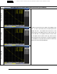
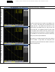
L M X 2 5 3 1 L Q 1 3 1 2 E E V A L U A T I O N B O A R D O P E R A T I N G I N S T R U C T I O N S Fractional Spurs (Internal Divide by 2 Disabled) Fractional Spur at 250 kHz offset at a worst case frequency of 1450.25 MHz is –72.7 dBc. Worst case channels occur at exactly one channel spacing above or below a multiple of the crystal frequency. Fractional Spur at 250 kHz offset at a worst case frequency of 1520.25 MHz is –69.4 dBc. Fractional Spur at 250 kHz offset at a worst case frequency of 1570.
L M X 2 5 3 1 L Q 1 3 1 2 E E V A L U A T I O N B O A R D O P E R A T I N G I N S T R U C T I O N S Fractional Spurs (Internal Divide by 2 Enabled) Spur at 250 kHz offset at a frequency of 595.125 MHz is –80.4 dBc. Since this mode uses the divide by 2 mode, the channel spacing here is actually 125 kHz. The spur at 125 kHz could be eliminated by doubling the channel spacing before the divider. Spur at 250 kHz offset for a frequency of 615.125 MHz is -85.7 dBc.
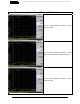
L M X 2 5 3 1 L Q 1 3 1 2 E E V A L U A T I O N B O A R D O P E R A T I N G I N S T R U C T I O N S Integer Spurs (Internal Divide by 2 Disabled) Spur at 10 MHz offset for a frequency of 1450 MHz is -83.7 dBc. Spur at 10 MHz offset for a frequency of 1520 MHz is below the spectrum analyzer noise floor. Spur at 10 MHz offset for a frequency of 1580 MHz is 92.0 dBc.
L M X 2 5 3 1 L Q 1 3 1 2 E E V A L U A T I O N B O A R D O P E R A T I N G I N S T R U C T I O N S Integer Spurs (Internal Divide by 2 Enabled) Spur at 10 MHz offset for a frequency of 725 MHz is below the spectrum analyzer noise floor. Spur at 10 MHz offset for a frequency of 707.5 MHz is below the spectrum analyzer noise floor. Spur at 10 MHz offset for a frequency of 790 MHz is below the spectrum analyzer noise floor.
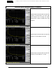
L M X 2 5 3 1 L Q 1 3 1 2 E E V A L U A T I O N B O A R D O P E R A T I N G I N S T R U C T I O N S CodeLoader Settings CodeLoader is designed to run many devices. When CodeLoader is first started, it is necessary to select the correct device.
L M X 2 5 3 1 L Q 1 3 1 2 E E V A L U A T I O N B O A R D O P E R A T I N G I N S T R U C T I O N S There can be different modes defined for a particular part. A mode can be recalled easily from the menu. This restores bit settings and frequencies, but not the Port Setup information. The default reference oscillator used for these instructions was 10 MHz, but there is an alternate mode for a 61.44 MHz oscillator as well.
L M X 2 5 3 1 L Q 1 3 1 2 E E V A L U A T I O N B O A R D O P E R A T I N G I N S T R U C T I O N S The Bits/Pins tab displays many of the bits used to program the part. Right mouse click any bit to view more information about what this does. When the DIV2 bit is enabled, the frequency from the part will be half of that shown on the PLL/VCO tab. The frequency on the PLL/VCO tab does not reflect this because the divide by 2 is actually after the VCO.
L M X 2 5 3 1 L Q 1 3 1 2 E E V A L U A T I O N B O A R D O P E R A T I N G I N S T R U C T I O N S The Registers tab shows the literal bits that are being sent to the part. These are the registers every time the PLL is loaded by using the menu command or (Ctrl+L). R5 (INIT1) and R5 (INIT 2) are just the R5 register being used to properly initialize the part. So a single (Ctrl+L) will load the part.
L M X 2 5 3 1 L Q 1 3 1 2 E E V A L U A T I O N B O A R D O P E R A T I N G I N S T R U C T I O N S The port setup tells CodeLoader what information goes where. If this is wrong, the part will not program. Although LPT1 is usually correct, CodeLoader does NOT automatically detect the correct port. On some laptops, it may be LPT3. Manual verification is required.
L M X 2 5 3 1 L Q 1 3 1 2 E E V A L U A T I O N B O A R D O P E R A T I N G I N S T R U C T I O N S Schematic 2 3 R2 2 4 6 8 R3 C1 R6 VccBUF D C3 VccPLL C7 C4 VccDIG R22 VccPLL R2pLF VregDI G NC GND Test OSCin* OSCin Ftest/LD NC Vr egPLL2 R24 C C18 VccDIG C10 C100 C11 R17 VccDIG NC GND NC NC VregBUF NC DATA CLK VccPLL VregPLL1 FLout CPout Vtune VccBUF Fout GND GND 27 26 25 24 23 22 21 20 19 LE CE NC NC NC NC VccVCO Vr egVCO Vr efVCO SLG1 SLG2 SLG3 R19 R10 R9 C8 C102 C15
L M X 2 5 3 1 L Q 1 3 1 2 E E V A L U A T I O N B O A R D O P E R A T I N G I N S T R U C T I O N S Bill of Materials Item QTY Bill of Materials Manufacturer Part # Size Tol Voltage LMX2531EB Material 20 Value Open Capacitors 0 n/a 6 C0G X7R X7R X5R X5R X5R Thick Film Thick Film Thick Film Thick Film Thick Film Thick Film Thick Film Thick Film Open Resistors Open Miscellaneous 100pF 0.010uF 0.10uF 1uF 4.7uF 10uF 0Ω 0.22Ω 3.
L M X 2 5 3 1 L Q 1 3 1 2 E E V A L U A T I O N B O A R D O P E R A T I N G Top Layer 19 I N S T R U C T I O N S
L M X 2 5 3 1 L Q 1 3 1 2 E E V A L U A T I O N B O A R D O P E R A T I N G I N S T R U C T I O N S Mid Layer 1 "Ground Plane" (15 Mils Down FR4) 20
L M X 2 5 3 1 L Q 1 3 1 2 E E V A L U A T I O N B O A R D O P E R A T I N G I N S T R U C T I O N S Mid Layer 2 "Power" 21
L M X 2 5 3 1 L Q 1 3 1 2 E E V A L U A T I O N B O A R D O P E R A T I N G I N S T R U C T I O N S Bottom Layer "Signal" Note: Total Board Thickness = 61 mils 22
L M X 2 5 3 1 L Q 1 3 1 2 E E V A L U A T I O N B O A R D O P E R A T I N G I N S T R U C T I O N S Top Build Diagram 23
IMPORTANT NOTICE Texas Instruments Incorporated and its subsidiaries (TI) reserve the right to make corrections, modifications, enhancements, improvements, and other changes to its products and services at any time and to discontinue any product or service without notice. Customers should obtain the latest relevant information before placing orders and should verify that such information is current and complete.