
Datasheet

LMZ10503
www.ti.com
SNVS641I –JANUARY 2010–REVISED OCTOBER 2013
LMZ10503 3A SIMPLE SWITCHER® Power Module with 5.5V Maximum Input Voltage
Check for Samples: LMZ10503
1
FEATURES
PERFORMANCE BENEFITS
2
• Integrated Shielded Inductor
• Operates at High Ambient Temperatures
• Flexible Startup Sequencing using External
• High Efficiency up to 96% Reduces System
Soft-Start, Tracking, and Precision Enable
Heat Generation
• Protection Against In-Rush Currents and
• Low Radiated Emissions (EMI) Complies with
Faults Such as Input UVLO and Output Short-
EN55022 Class B Standard
(2)
Circuit
• Low Output Voltage Ripple of 10 mV Allows
• -40°C to +125°C Junction Temperature
for Powering Noise-Sensitive Transceiver and
Operating Range
Signaling ICs
• Single Exposed pad and Standard Pinout for
• Fast Transient Response for Powering FPGAs
Easy Mounting and Manufacturing
and ASICs
• Pin-to-Pin Compatible with
– LMZ10504 (4A/20W max)
ELECTRICAL SPECIFICATIONS
– LMZ10505 (5A/25W max)
• 15W Maximum Total Output Power
• Fully Enabled for WEBENCH® and Power
• Up to 3A Output Current
Designer
• Input Voltage Range 2.95V to 5.5V
• Output Voltage Range 0.8V to 5V
APPLICATIONS
• ±1.63% Feedback Voltage Accuracy Over
• Point-of-Load Conversions from 3.3V and 5V
Temperature
Rails
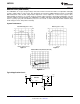
• Efficiency up to 96%
• Space Constrained Applications
• Extreme Temperatures/no Air Flow
DESCRIPTION
Environments
The LMZ10503 SIMPLE SWITCHER® power module
• Noise Sensitive Applications (i.e. Transceiver,
is a complete, easy-to-use DC-DC solution capable of
Medical)
driving up to a 3A load with exceptional power
conversion efficiency, output voltage accuracy, line
and load regulation. The LMZ10503 is available in an
innovative package that enhances thermal
performance and allows for hand or machine
soldering.
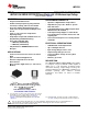
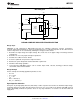
Figure 1. Easy to use PFM 7 Pin Package
10.16 x 13.77 x 4.57 mm (0.4 x 0.39 x 0.18 in)
θ
JA
= 20°C/W, θ
JC
= 1.9°C/W
(1)
RoHS Compliant
Peak Reflow Case Temp = 245°C
Power Module SMT Guidelines
(1) θ
JA
measured on a 2.25” x 2.25” (5.8 cm x 5.8 cm) four layer
board, with one ounce copper, thirty six thermal vias, no air
flow, and 1W power dissipation. Refer to PCB Layout
Diagrams or Evaluation Board Application Note: AN-2022 (2) EN 55022:2006, +A1:2007, FCC Part 15 Subpart B: 2007.
(SNVA421). See Table 9 and layout for information on device under test.
1
Please be aware that an important notice concerning availability, standard warranty, and use in critical applications of
Texas Instruments semiconductor products and disclaimers thereto appears at the end of this data sheet.
2All trademarks are the property of their respective owners.
PRODUCTION DATA information is current as of publication date.
Copyright © 2010–2013, Texas Instruments Incorporated
Products conform to specifications per the terms of the Texas
Instruments standard warranty. Production processing does not
necessarily include testing of all parameters.