
Datasheet
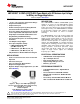
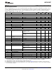
Table Of Contents
- FEATURES
- APPLICATIONS
- DESCRIPTION
- Electrical Specifications
- Performance Benefits
- Absolute Maximum Ratings
- Operating Ratings
- Electrical Characteristics
- Typical Performance Characteristics
- Application Block Diagram
- Revision History
LMZ14202EXT
www.ti.com
SNVS665F –JUNE 2010–REVISED OCTOBER 2013
LMZ14202EXT 2A SIMPLE SWITCHER® Power Module with 42V Maximum Input Voltage
for Military and Rugged Applications
Check for Samples: LMZ14202EXT
1
FEATURES
DESCRIPTION
2
• – 55°C to 125°C Junction Temperature Range
The LMZ14202EXT SIMPLE SWITCHER® power
• Integrated Shielded Inductor
module is an easy-to-use step-down DC-DC solution
capable of driving up to 2A load with exceptional
• Simple PCB Layout
power conversion efficiency, line and load regulation,
• Flexible Startup Sequencing Using External
and output accuracy. The LMZ14202EXT is available
Soft-Start and Precision Enable
in an innovative package that enhances thermal
• Protection Against Inrush Currents and Faults
performance and allows for hand or machine
such as Input UVLO and Output Short Circuit
soldering.
• Single Exposed Pad and Standard Pinout for
The LMZ14202EXT can accept an input voltage rail
Easy Mounting and Manufacturing
between 6V and 42V and deliver an adjustable and
highly accurate output voltage as low as 0.8V. The
• Fast Transient Response for Powering FPGAs
LMZ14202EXT only requires three external resistors
and ASICs
and four external capacitors to complete the power
• Low Output Voltage Ripple
solution. The LMZ14202EXT is a reliable and robust
• Pin-to-pin Compatible Family:
design with the following protection features: thermal
shutdown, input under-voltage lockout, output over-
– LMZ14203EXT/2EXT/1EXT
voltage protection, short-circuit protection, output
(42V Max 3A, 2A, 1A)
current limit, and allows startup into a pre-biased
– LMZ14203/2/1 (42V Max 3A, 2A, 1A)
output. A single resistor adjusts the switching
– LMZ12003/2/1 (20V Max 3A, 2A, 1A)
frequency up to 1 MHz.
• Fully Enabled for Webench® Power Designer
ELECTRICAL SPECIFICATIONS
APPLICATIONS
• 12W Maximum Total Output Power
• Point of Load Conversions from 12V and 24V
• Up to 2A Output Current
Input Rail
• Input Voltage Range 6V to 42V
• Time Critical Projects
• Output Voltage Range 0.8V to 6V
• Space Constrained / High Thermal
• Efficiency up to 90%
Requirement Applications
• Negative Output Voltage Applications (See AN-
PERFORMANCE BENEFITS
2027 SNVA425)
• Low Radiated Emissions / High Radiated
Immunity
• Passes Vibration Standard MIL-STD-883
Method 2007.2 Condition A JESD22–B103B
Condition 1
• Passes Drop Standard MIL-STD-883 Method
2002.3 Condition B JESD22–B110 Condition B
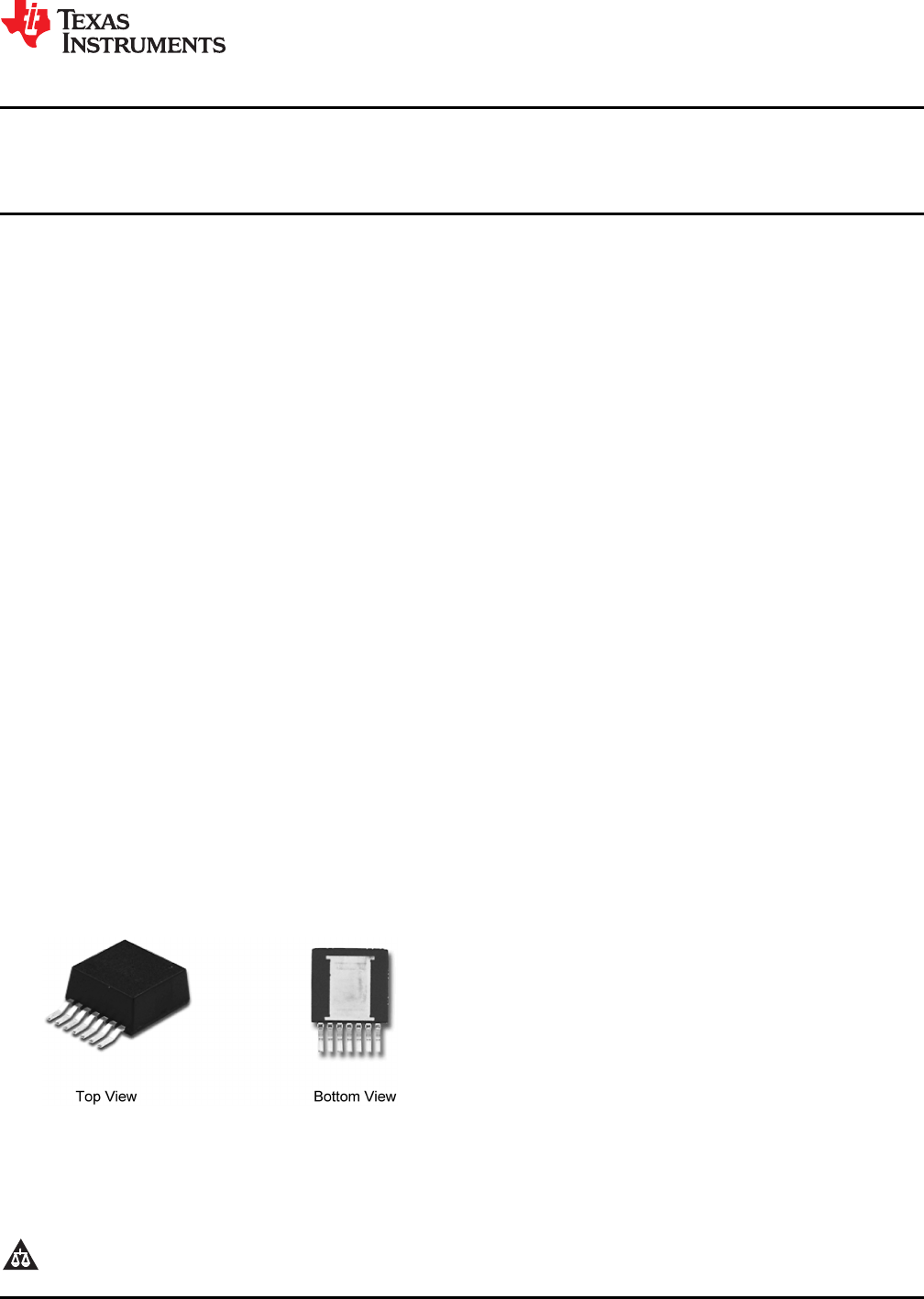
Figure 1. Easy to use PFM 7 pin package
10.16 x 13.77 x 4.57 mm (0.4 x 0.542 x 0.18 in)
θ
JA
= 20°C/W, θ
JC
= 1.9°C/W
RoHS Compliant
Peak Reflow Case Temp = 245°C
Power Module SMT Guidelines
1
Please be aware that an important notice concerning availability, standard warranty, and use in critical applications of
Texas Instruments semiconductor products and disclaimers thereto appears at the end of this data sheet.
2All trademarks are the property of their respective owners.
PRODUCTION DATA information is current as of publication date.
Copyright © 2010–2013, Texas Instruments Incorporated
Products conform to specifications per the terms of the Texas
Instruments standard warranty. Production processing does not
necessarily include testing of all parameters.