
Datasheet
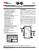


50
55
60
65
70
75
80
85
90
95
100
0 4 8 12 16 20
Efficiency (%)
Output Current (A)
PVIN = 3.3 V, VIN = 5 V
PVIN = VIN = 5 V
PVIN = VIN = 12 V
C001
Vout = 1.8 V
Fsw = 500 kHz
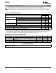
VOUT
AGND
SENSE+
LMZ31520
FREQ_SEL
SS_SEL
V5V
C
O
C
I
VIN
VIN
VOUT
PGND
VADJ
R
SET
ILIM
INH
PWRGD
PVIN
LMZ31520
www.ti.com
SLVSBM9B –OCTOBER 2013–REVISED DECEMBER 2013
20A SIMPLE SWITCHER® Power Module with 3.0V-14.5V Input in QFN Package
Check for Samples: LMZ31520
1
FEATURES
DESCRIPTION
2
• Complete Integrated Power Solution;
The LMZ31520 SIMPLE SWITCHER® power module
Smaller than a Discrete Design
is an easy-to-use integrated power solution that
• 15 mm × 16 mm × 5.8 mm Package Size
combines a 20-A DC/DC converter with power
- Pin Compatible with LMZ31530
MOSFETs, a shielded inductor, and passives into a
• Ultra-Fast Load Step Response
low profile, QFN package. This total power solution
allows as few as three external components and
• Efficiencies Up To 96%
eliminates the loop compensation and magnetics part
• Wide-Output Voltage Adjust
selection process.
0.6 V to 3.6 V, with 1% Reference Accuracy
The 15x16x5.8 mm QFN package is easy to solder
• Optional Split Power Rails Allows
onto a printed circuit board and allows a compact
Input Voltage Down to 3.0 V
point-of-load design. Achieves greater than 95%
• Selectable Switching Frequency
efficiency, has ultra-fast load step response and
(300 kHz to 850 kHz)
excellent power dissipation capability with a thermal
impedance of 8.6°C/W. The LMZ31520 offers the
• Selectable Slow-Start
flexibility and the feature-set of a discrete point-of-
• Adjustable Overcurrent Limit
load design and is ideal for powering a wide range of
• Power Good Output
ICs and systems. Advanced packaging technology
affords a robust and reliable power solution
• Output Voltage Sequencing
compatible with standard QFN mounting and testing
• Over Temperature Protection
techniques.
• Pre-bias Output Start-up
SIMPLIFIED APPLICATION
• Operating Temperature Range: –40°C to 85°C
• Enhanced Thermal Performance: 8.6°C/W
• Meets EN55022 Class A Emissions
- Integrated Shielded Inductor
APPLICATIONS
• Broadband and Communications
Infrastructure
• DSP and FPGA Point of Load Applications
• High Density Power Systems
1
Please be aware that an important notice concerning availability, standard warranty, and use in critical applications of
Texas Instruments semiconductor products and disclaimers thereto appears at the end of this data sheet.
2 is a trademark of ~ Texas Instruments.
PRODUCTION DATA information is current as of publication date.
Copyright © 2013, Texas Instruments Incorporated
Products conform to specifications per the terms of the Texas
Instruments standard warranty. Production processing does not
necessarily include testing of all parameters.