
Datasheet
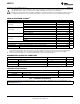
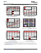
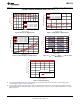

50
55
60
65
70
75
80
85
90
95
100
0 1 2 3 4 5 6 7 8 9 10
Efficiency (%)
Output Current (A)
PVIN = 3.3 V, VIN = 5 V
PVIN = VIN = 5 V
PVIN = VIN = 12 V
C001
Vout = 2.5 V
Fsw = 750 kHz
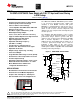
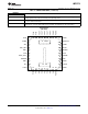
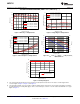
LMZ31710
PWRGD
SENSE+
VOUT
PVIN
VIN
INH/UVLO
RT/CLK
VADJ
SS/TR
STSEL
AGND PGND
C
IN
R
SET
C
OUT
V
OUT
V
IN
R
RT
SYNC_OUT
ISHARE
LMZ31710
www.ti.com
SNVS987A –JULY 2013–REVISED JULY 2013
10A SIMPLE SWITCHER® Power Module with 2.95V-17V Input and Current Sharing
in QFN Package
Check for Samples: LMZ31710
1
FEATURES
DESCRIPTION
The LMZ31710 SIMPLE SWITCHER power module
2
• Complete Integrated Power Solution Allows
is an easy-to-use integrated power solution that
Small Footprint, Low-Profile Design
combines a 10-A DC/DC converter with power
• 10mm x 10mm x 4.3mm Package
MOSFETs, a shielded inductor, and passives into a
- Pin Compatible with LMZ31707 & LMZ31704
low profile, QFN package. This total power solution
allows as few as three external components and
• Efficiencies Up to 95%
eliminates the loop compensation and magnetics part
• Eco-Mode / Light Load Efficiency (LLE)
selection process.
• Wide-Output Voltage Adjust
The 10x10x4.3 mm QFN package is easy to solder
0.6 V to 5.5 V, with 1% Reference Accuracy
onto a printed circuit board and allows a compact
• Supports Parallel Operation for Higher Current
point-of-load design. Achieves greater than 95%
• Optional Split Power Rail allows
efficiency and excellent power dissipation capability
Input Voltage Down to 2.95 V
with a thermal impedance of 13.3°C/W. The
LMZ31710 offers the flexibility and the feature-set of
• Adjustable Switching Frequency
a discrete point-of-load design and is ideal for
(200 kHz to 1.2 MHz)
powering a wide range of ICs and systems.
• Synchronizes to an External Clock
Advanced packaging technology affords a robust and
• Provides 180° Out-of-Phase Clock Signal
reliable power solution compatible with standard QFN
mounting and testing techniques.
• Adjustable Slow-Start
• Output Voltage Sequencing / Tracking
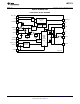
Figure 1. SIMPLIFIED APPLICATION
• Power Good Output
• Programmable Undervoltage Lockout (UVLO)
• Over-Current & Over-Temperature Protection
• Pre-bias Output Start-up
• Operating Temperature Range: –40°C to 85°C
• Enhanced Thermal Performance: 13.3°C/W
• Meets EN55022 Class B Emissions
- Integrated Shielded Inductor
APPLICATIONS
• Broadband & Communications Infrastructure
• Automated Test and Medical Equipment
• Compact PCI / PCI Express / PXI Express
• DSP and FPGA Point-of-Load Applications
1
Please be aware that an important notice concerning availability, standard warranty, and use in critical applications of
Texas Instruments semiconductor products and disclaimers thereto appears at the end of this data sheet.
2All trademarks are the property of their respective owners.
PRODUCTION DATA information is current as of publication date.
Copyright © 2013, Texas Instruments Incorporated
Products conform to specifications per the terms of the Texas
Instruments standard warranty. Production processing does not
necessarily include testing of all parameters.