
Datasheet

using: The value of θ
JA
for the SOT-23 package is 220°C/W. Exceeding the maximum allowable power dissipation will
LP2982
SNVS128J –MARCH 2000–REVISED APRIL 2013
www.ti.com
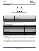
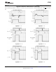
Connection Diagram
Top View
Figure 1. 5-Lead Small Outline SOT-23 Package
See Package Number DBV0005A
Pin Descriptions
Name Pin Number Function
V
IN
1 Input Voltage
GND 2 Common Ground (device substrate)
ON/OFF 3 Logic high enable input
BYPASS 4 Bypass capacitor for low noise operation
V
OUT
5 Regulated output voltage
These devices have limited built-in ESD protection. The leads should be shorted together or the device placed in conductive foam
during storage or handling to prevent electrostatic damage to the MOS gates.
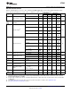
Absolute Maximum Ratings
(1)(2)
Storage Temperature Range −65°C to +150°C
Operating Junction Temperature Range −40°C to +125°C
Lead Temperature (Soldering, 5 sec.) 260°C
ESD Rating
(3)
2 kV
Power Dissipation
(4)
Internally Limited
Input Supply Voltage (Survival) −0.3V to +16V
Input Supply Voltage (Operating) 2.1V to +16V
Shutdown Input Voltage (Survival) −0.3V to +16V
Output Voltage (Survival
(5)
) −0.3V to +9V
I
OUT
(Survival) Short Circuit Protected
Input-Output Voltage (Survival
(6)
) −0.3V to +16V
(1) Absolute maximum ratings indicate limits beyond which damage to the component may occur. Electrical specifications do not apply
when operating the device outside of its rated operating conditions.
(2) If Military/Aerospace specified devices are required, please contact the Texas Instruments Sales Office/Distributors for availability and
specifications.
(3) The ESD rating of pins 3 and 4 for the SOT-23 package, or pins 5 and 2 for the DSBGA package, is 1 kV.
(4) The maximum allowable power dissipation is a function of the maximum junction temperature, T
J(MAX)
, the junction-to-ambient thermal
resistance, θ
JA
, and the ambient temperature, T
A
. The maximum allowable power dissipation at any ambient temperature is calculated
cause excessive die temperature, and the regulator will go into thermal shutdown.
(5) If used in a dual-supply system where the regulator load is returned to a negative supply, the LP2982 output must be diode-clamped to
ground.
(6) The output PNP structure contains a diode between the V
IN
and V
OUT
terminals that is normally reverse-biased. Reversing the polarity
from V
IN
to V
OUT
will turn on this diode. (See REVERSE CURRENT PATH.)
2 Submit Documentation Feedback Copyright © 2000–2013, Texas Instruments Incorporated
Product Folder Links: LP2982