
Datasheet

LP2992
www.ti.com
SNVS171G –NOVEMBER 2001–REVISED MARCH 2013
These devices have limited built-in ESD protection. The leads should be shorted together or the device placed in conductive foam
during storage or handling to prevent electrostatic damage to the MOS gates.
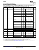
Absolute Maximum Ratings
(1)(2)
Storage Temperature Range −65°C to +150°C
Operating Junction Temperature Range −40°C to +125°C
Lead Temp. (Soldering, 5 sec.) 260°C
ESD Rating
(3)
2 kV
Power Dissipation
(4)
Internally Limited
Input Supply Voltage (Survival) −0.3V to +16V
Input Supply Voltage (Operating) 2.2V to +16V
Shutdown Input Voltage (Survival) −0.3V to +16V
Output Voltage (Survival,
(5)
) −0.3V to +9V
I
OUT
(Survival) Short Circuit Protected
Input-Output Voltage (Survival,
(6)
) −0.3V to +16V
(1) “Absolute Maximum Ratings” indicate limits beyond which damage to the component may occur. Electrical specifications do not apply
when operating the device outside of its rated operating conditions.
(2) If Military/Aerospace specified devices are required, please contact the Texas Instruments Sales Office/Distributors for availability and
specifications.
(3) The ESD rating of pins 3 and 4 for the SOT-23 package, or pins 1 and 3 for the WSON package, is 1 kV.
(4) The maximum allowable power dissipation is a function of the maximum junction temperature, T
J
(MAX), the junction-to-ambient thermal
resistance, θ
J-A
, and the ambient temperature, T
A
. The maximum allowable power dissipation at any ambient temperture is calculated
using:
Where the value of θ
J-A
for the SOT-23 package is 220°C/W in a typical PC board mounting and the WSON package is 65°C/W.
Exceeding the maximum allowable dissipation will cause excessive die temperature, and the regulator will go into thermal shutdown.
(5) If used in a dual-supply system where the regulator load is returned to a negative supply, the LP2992 output must be diode-clamped to
ground.
(6) The output PNP structure contains a diode between the V
IN
to V
OUT
terminals that is normally reverse-biased. Reversing the polarity
from V
IN
to V
OUT
will turn on this diode.
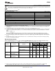
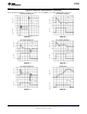
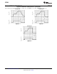
Electrical Characteristics
Limits in standard typeface are for T
J
= 25°C. and limits in boldface type apply over the full operating temperature range.
Unless otherwise specified: V
IN
= V
O
(NOM) + 1V, I
L
= 1 mA, C
IN
= 1 µF, C
OUT
= 4.7 µF, V
ON/OFF
= 2V.
LP2992AI-X.X LP2992I-X.X
Symbol Parameter Conditions Typ
(1) (1)
Units
Min Max Min Max
ΔV
O
Output Voltage I
L
= 1 mA −1.0 1.0 −1.5 1.5
Tolerance
1 mA ≤ I
L
≤ 50 mA −1.5 1.5 −2.5 2.5
−2.5 2.5 −3.5 3.5 %V
NOM
1 mA ≤ I
L
≤ 250 mA −3.5 3.5 −4.0 4.0
−4.5 4.5 −5.0 5.0
ΔV
O
/ΔV
IN
Output Voltage V
O
(NOM)+1V ≤ V
IN
≤ 16V 0.007 0.014 0.014
%/V
Line Regulation 0.032 0.032
V
IN
(min) Minimum input voltage 2.05 2.20 2.20 V
required to maintain
output regulation
(1) Limits are 100% production tested at 25°C. Limits over the operating temperature range are specified through correlation using
Statistical Quality Control (SQC) methods. The limits are used to calculate TI's Average Outgoing Quality Level (AOQL).
Copyright © 2001–2013, Texas Instruments Incorporated Submit Documentation Feedback 3
Product Folder Links: LP2992