
Datasheet

LP2992
SNVS171G –NOVEMBER 2001–REVISED MARCH 2013
www.ti.com
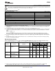
Electrical Characteristics (continued)
Limits in standard typeface are for T
J
= 25°C. and limits in boldface type apply over the full operating temperature range.
Unless otherwise specified: V
IN
= V
O
(NOM) + 1V, I
L
= 1 mA, C
IN
= 1 µF, C
OUT
= 4.7 µF, V
ON/OFF
= 2V.
LP2992AI-X.X LP2992I-X.X
Symbol Parameter Conditions Typ
(1) (1)
Units
Min Max Min Max
V
IN
–V
O
Dropout Voltage I
L
= 0 0.5 2.5 2.5
(2)
4 4
I
L
= 1 mA 5 9 9
12 12
I
L
= 50 mA 100 125 125
mV
180 180
I
L
= 150 mA 260 325 325
470 470
I
L
= 250 mA 450 575 575
850 850
I
GND
Ground Pin Current I
L
= 0 65 95 95
125 125
I
L
= 1 mA 75 110 110
170 170
I
L
= 50 mA 350 600 600
1000 1000
µA
I
L
= 150 mA 850 1500 1500
2500 2500
I
L
= 250 mA 1500 2300 2300
4000 4000
V
ON/OFF
< 0.3V 0.01 0.8 0.8
V
ON/OFF
< 0.15V 0.05 2 2
V
ON/OFF
ON/OFF Input Voltage High = O/P ON 1.4 1.6 1.6
V
(3)
Low = O/P OFF 0.55 0.15 0.15
I
ON/OFF
ON/OFF Input Current V
ON/OFF
= 0 0.01 −2 −2
µA
V
ON/OFF
= 5V 5 15 15
e
n
Output Noise BW = 300 Hz to 50 kHz,
Voltage (RMS) C
OUT
= 10 µF 30 µV
C
BYPASS
= 10 nF
ΔV
OUT
/ΔV
IN
Ripple Rejection f = 1 kHz, C
BYPASS
= 10 nF
45 dB
C
OUT
= 10 µF
I
O
(SC) Short Circuit Current R
L
= 0 (Steady State)
400 mA
(4)
I
O
(PK) Peak Output Current V
OUT
≥ V
o
(NOM) −5% 350 mA
(2) V
IN
must be the greater of 2.2V or V
OUT(nom)
+ Dropout Voltage to maintain output regulation. Dropout voltage is defined as the input to
output differential at which the output voltage drops 2% below the value measured with a 1V differential.
(3) The ON/OFF input must be properly driven to prevent possible misoperation. For details, refer to Application Hints.
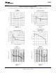
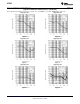
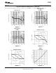
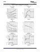
(4) The LP2992 has foldback current limiting which allows a high peak current when V
OUT
> 0.5V, and then reduces the maximum output
current as V
OUT
is forced to ground (see Typical Performance Characteristics curves).
4 Submit Documentation Feedback Copyright © 2001–2013, Texas Instruments Incorporated
Product Folder Links: LP2992