
Datasheet
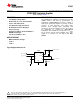
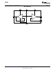

V
TT
LP2995
PV
IN
V
DDQ
V
REF
AV
IN
V
REF
=
1.25V
+
V
SENSE
GND
50PF
+
+
V
DDQ
=
2.5V
V
DD
=
2.5V
V
TT
=
1.25V
220PF
0.1PF
LP2995
www.ti.com
SNVS190M –FEBRUARY 2002–REVISED MARCH 2013
LP2995 DDR Termination Regulator
Check for Samples: LP2995
1
FEATURES
DESCRIPTION
The LP2995 linear regulator is designed to meet the
2
• Low Output Voltage Offset
JEDEC SSTL-2 and SSTL-3 specifications for
• Works with +5v, +3.3v and 2.5v Rails
termination of DDR-SDRAM. The device contains a
• Source and Sink Current
high-speed operational amplifier to provide excellent
response to load transients. The output stage
• Low External Component Count
prevents shoot through while delivering 1.5A
• No External Resistors Required
continuous current and transient peaks up to 3A in
• Linear Topology
the application as required for DDR-SDRAM
termination. The LP2995 also incorporates a V
SENSE
• Available in SOIC-8, SO PowerPAD-8 or
pin to provide superior load regulation and a V
REF
WQFN-16 Packages
output as a reference for the chipset and DDR
• Low Cost and Easy to Use
DIMMS.
WHITE SPACE
APPLICATIONS
WHITE SPACE
• DDR Termination Voltage
• SSTL-2
WHITE SPACE
• SSTL-3
WHITE SPACE
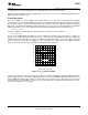
Typical Application Circuit
1
Please be aware that an important notice concerning availability, standard warranty, and use in critical applications of
Texas Instruments semiconductor products and disclaimers thereto appears at the end of this data sheet.
2All trademarks are the property of their respective owners.
PRODUCTION DATA information is current as of publication date.
Copyright © 2002–2013, Texas Instruments Incorporated
Products conform to specifications per the terms of the Texas
Instruments standard warranty. Production processing does not
necessarily include testing of all parameters.