
Datasheet

Selecting C
FF
www.ti.com
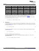
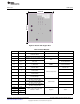
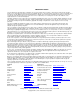
Table 1. Suggested Components
V
OUT
R1 R2 C
FF
F
Z
0.80 V 1.07 kΩ 1.78 kΩ 4700 pF 31.6 kHz
1.00 V 1.00 kΩ 1.00 kΩ 4700 pF 33.8 kHz
1.20 V 1.40 kΩ 1.00 kΩ 3300 pF 34.4 kHz
1.50 V 2.00 kΩ 1.00 kΩ 2700 pF 29.5 kHz
1.80 V 2.94 kΩ 1.13 kΩ 1500 pF 36.1 kHz
2.00 V 1.02 kΩ 340Ω 4700 pF 33.2 kHz
2.50 V 1.02 kΩ 255Ω 4700 pF 33.2 kHz
3.00 V 1.00 kΩ 200Ω 4700 pF 33.8 kHz
3.30 V 2.00 kΩ 357Ω 2700 pF 29.5 kHz
For additional information on how resistor tolerances affect the calculated V
OUT
value, see AN-1378
Method for Calculating Output Voltage Tolerances in Adjustable Regulators (SNVA112).
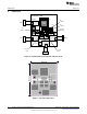
The LP38512TJ-ADJ evaluation board is assembled with a 1.40 kΩ ±1% resistor for R1, and a 1.00 kΩ
±1% resistor for R2. This sets V
OUT
to 1.20 V.
V
OUT
= 500 mV x (1 + (1.40 kΩ / 1.00 kΩ) ) = 1.20 V (3)
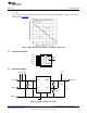
5 Selecting C
FF
A capacitor placed across the gain resistor R1 provides additional phase margin to improve load transient
response of the device. This capacitor, C
FF
, in parallel with R1, forms a zero in the loop response given by
the formula in Equation 4:
F
Z
= (1 / (2 x π x C
FF
x R1) ) (4)
The value for C
FF
should be selected to set a zero frequency (F
Z
) between 25 kHz and 50 kHz using the
formula in Equation 5:
C
FF
= 1 / (2 x π x F
Z
x R1) (5)
The closest standard 10% value is adequate for C
FF
.
The LP38512TJ-ADJ Evaluation board is assembled with a 3300 pF capacitor for C
FF
. This sets F
Z
to
approximately 34 kHz.
F
Z
= (1 / (2 x π x 3300 pF x 1.40 kΩ ) ) = 34.4 kHz (6)
2
AN-1802 LP38512TJ-ADJ Evaluation Board SNVA331B–January 2009–Revised April 2013
Submit Documentation Feedback
Copyright © 2009–2013, Texas Instruments Incorporated