
Datasheet


Enable Function
www.ti.com
6 Enable Function
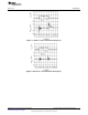
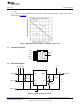
ON/OFF control is provided by supplying a logic level signal to the Enable pin. A minimum V
EN
value of 1.2
V is typically required at this pin to enable the LDO output. The LDO output will be shutdown when the V
EN
value is typically 0.6 V or less. The V
EN
threshold incorporates approximately 100 mV of hysteresis.
Figure 3. V
OUT
vs V
EN
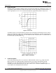
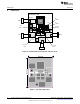
The Enable pin has no internal default bias and must not be left floating. The Enable pin must be actively
driven to the appropriate voltage level. In applications where the LP38513TJ is operated continuously, the
Enable pin can be connected directly to V
IN
. The LP38512TJ-ADJ evaluation board is assembled with a 10
kΩ resistor (R3) to provide pull-up to V
IN
.
Figure 4. Enable Thresholds
7 Power Dissipation
The TO-263 THIN package alone has a junction to ambient thermal resistance (θ
JA
) rating of 67°C/W.
When mounted on the LP38512TJ-ADJ evaluation board, the θ
JA
rating is approximately 35°C/W.
Although there is only approximately 0.20 square inches (0.45in x 0.45in) of 1 ounce copper area
immediately under the package body, the top copper surface area is extended to additional copper area
on the bottom of the board by fifteen thermal vias.
4
AN-1802 LP38512TJ-ADJ Evaluation Board SNVA331B–January 2009–Revised April 2013
Submit Documentation Feedback
Copyright © 2009–2013, Texas Instruments Incorporated