
Datasheet


LP395
SNOSBF3C –APRIL 1998–REVISED MARCH 2013
www.ti.com
These devices have limited built-in ESD protection. The leads should be shorted together or the device placed in conductive foam
during storage or handling to prevent electrostatic damage to the MOS gates.
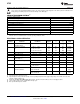
ABSOLUTE MAXIMUM RATINGS
(1)
Collector to Emitter Voltage 36V
Collector to Base Voltage 36V
Base to Emitter Voltage (Forward) 36V
Base to Emitter Voltage (Reverse) 10V
Base to Emitter Current (Reverse) 20 mA
Collector Current Limit Internally Limited
Power Dissipation Internally Limited
Operating Temperature Range −40°C to +125°C
Storage Temperature Range −65°C to +150°C
Lead Temp. (Soldering, 10 seconds) 260°C
(1) Absolute Maximum Ratings indicate limits beyond which damage to the device may occur. Operating Ratings indicate conditions for
which the device is functional, but do not ensure specific performance limits.
ELECTRICAL CHARACTERISTICS
Tested Limit Design Limit Units
Symbol Parameter Conditions Typical
(1) (2)
(Limit)
V
CE
Collector to Emitter 0.5 mA ≤ I
C
≤ 100 mA 36 36 V(Max)
Operating Voltage
(3)
I
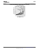
CL
Collector Current Limit V
BE
= 2V, V
CE
= 36V 45 25 20 mA(Min)
(4)
V
BE
= 2V, V
CE
= 15V 90 60 50 mA(Min)
V
BE
= 2V, 2V ≤ V
CE
≤ 6V 130 100 100 mA(Min)
I
B
Base Current 0 ≤ I
C
≤ 100 mA −0.3 −2.0 −2.5 μA(Max)
I
Q
Quiescent Current V
BE
= 0V, 0 ≤ V
CE
≤ 36V 0.24 0.50 0.60 mA(Max)
V
CE(SAT)
Saturation Voltage V
BE
= 2V, I
C
= 100 mA 1.82 2.00 2.10 V(Max)
BV
BE
Base to Emitter Break- 0 ≤ V
CE
≤ 36V, I
B
= 2 μA 36 36 V(Min)
down Voltage
(4)
V
BE
Base to Emitter Voltage I
C
= 5 mA 0.69 0.79 0.90 V(Max)
(5)
I
C
= 100 mA
(4)
1.02 1.40 V (Max)
t
S
Switching Time V
CE
= 20V, R
L
= 200Ω 2 μs
V
BE
= 0V, +2V, 0V
θ
JA
Thermal Resistance 0.4″ leads soldered to 150 180 °C/W
Junction to Ambient printed circuit board (Max)
0.125″ leads soldered to 130 160 °C/W
printed circuit board (Max)
(1) Specified and 100% production tested.
(2) Specified (but not 100% production tested) over the operating temperature and supply voltage ranges. These limits are not used to
calculate outgoing quality levels.
(3) Parameters identified with boldface type apply at temp. extremes. All other numbers, unless noted apply at +25°C.
(4) These numbers apply for pulse testing with a low duty cycle.
(5) Base positive with respect to emitter.
2 Submit Documentation Feedback Copyright © 1998–2013, Texas Instruments Incorporated
Product Folder Links: LP395